MICRO
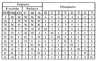
UNIT – 7Memory Interface – 2, I/O Interface – 1 Q1) Explain the 3:8 decoder IC?A1) The 3-to-8 Line Decoder (74LS138) One of the more common, although not only, integrated circuit decoders found in many microprocessor-based systems is the 74LS138 3-to-8line decoder. The figure below shows this decoder and its truth table. The truth table shows that only one of the eight outputs ever goes low at any time. For any of the decoder's outputs to go low, the three enable inputs (G2A, G2B, and Gl) must all be active. To be active, the G2A and G2B inputs must both be low (logic 0), and G I must be high (logic 1). Once the 74LS138 is enabled, the address inputs (C, B, and A) select which output pin goes low. Imagine eight EPROM CE inputs connected to the eight outputs of the decoder! This is a very powerful device because it selects eight different memory devices at the same time.
Fig 1 3:8 Decoder
Fig 2 Truth Table for 3:8 Decoder Q2) Explain dual 2-to-4 line decoder?A2) Another decoder that finds some application is the 74LS139 dual 2-to-4line decoder. Figure below shows both the pin-out and the truth table for this decoder. The 74LS139 contains two separate 2-to-4line decoders--each with its own address, enable, and output connections.
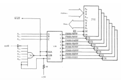
Fig 3 2 to 4line Decoder ad its Truth Table Q3) What are PLDs?A3) This section of the text explains the use of the programmable logic device or PLD as a decoder. Recently, the PAL has replaced PROM address decoders in the latest memory interfaces. There are three PLD devices that function in basically the same manner, but have different names: PLA (programmable logic array), PAL (programmable array logic), and GAL (gated array logic). Although these devices have been in existence since the mid-1970s, they have only recently appeared in memory systems and digital designs. The PAL and the PLA are fuse programmed, as is the PROM, and some PLD devices are erasable, as are EPROMs. In essence, all three devices are arrays of logic elements that are programmable. Q4) What are combinatorial PLAs?A4) One of the two basic types of PALs is the combinatorial programmable logic array. This device is internally structured as a programmable array of combinational logic circuits. This device, which is very common, has 10 fixed inputs, 2 fixed outputs, and 6 pins that are programmable as inputs or outputs. Each output pin is generated from a 7-input OR gate that has an AND gate attached to each input. The outputs of the OR gates pass through a three-state inverter that defines each out as an AND/NOR function. Initially, all of the fuses connect all of the vertical/horizontal connections. Programming is accomplished by blowing fuses to connect various inputs to the OR gate array. The wired-AND function is performed at each input connection that allows a product term of up to 16 inputs. A logic expression using the PAL16L8 can have 7 product terms with 16 inputs NORed together to generate the output expression. This device is ideal as a memory address decoder because of its structure. It is also ideal because the outputs are active low. Q5) Explain memory interfacing of EPROM with 8086?A5) Figure below shows an 8088-microprocessor connected to eight 2732 EPROMs, 4K x 8 memory devices that are in very common use today. The 2732 has one more address input (A 11) than the 2716, and twice the memory. The device in this illustration decodes eight 4K x 8 blocks of memory, for a total of 32K x 8 bits of the physical address space for the 8088. The decoder (74LS138) is connected a little differently than might be expected because the slower version of this type of EPROM has a memory access time of 450 ns. Recall from Chapter 8 that when the 8088 is operated with a 5 MHz clock, it allows 460 ns for the memory to access data. Because of the decoder's added time delay (12 ns), it is impossible for this memory to function within 460 ns. In order to correct this problem, we must add a NAND gate to generate a signal to enable the decoder and a signal for the wait state generator. With a wait state inserted every time this section of the memory is accessed, the 8088 will allow 660 ns for the EPROM to access data. Recall that an extra wait state adds 200 ns (1 clock) to the access time. The 660 ns is ample time for a 450 ns memory component to access data, even with the delays introduced by the decoder and any buffers added to the data bus.
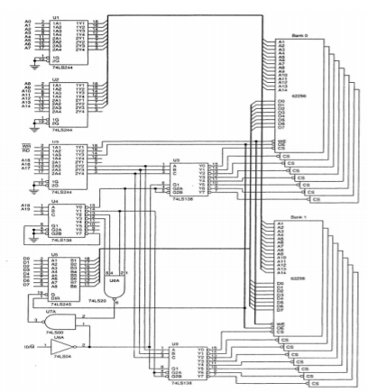
Fig 4 8 EPROM interfaced to 8088-microprocessor The decoder is selected for a memory address range that begins at location F8000H and continues through location FFFFFH-the upper 32K bytes of memory. This section of memory is an EPROM because FFFFOH is where the 8088 starts to execute instructions after a hardware reset. We often call location FFFFOH the cold-start location. The software stored in this section of memory would contain a JMP instruction at location FFFFOH that jumps to location F8000H so that the remainder of the program can execute. Q6) Explain Interfacing RAM to the 8088?A6) RAM is a little easier to interface than EPROM because most RAM memory components do not require wait states. An ideal section of the memory for the RAM is the very bottom, which contains vectors for interrupts. Interrupt vectors are often modified by software packages, so it is rather important to encode this section of the memory with RAM. In the below figure sixteen 62256 32K x 8 static RAMS are interfaced to the 8088, beginning at memory location OOOOOH. This circuit board uses two decoders to select the sixteen different RAM memory components and a third to select the other decoders for the appropriate memory sections. Sixteen 32K RAMs fill memory from location OOOOOH through location 7FFFFH, for 512K bytes of memory. The first decoder (U4) in this circuit selects the other two decoders. An address beginning with 00: selects decoder U3, and an address that begins with 0 I select decoder U9. Notice that extra pins remain at the output of decoder U4 for future expansion. These allow more 256K x 8 blocks of RAM, for a total of l M x 8, simply by adding the RAM and the additional secondary decoders.
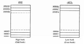
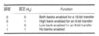
Fig 5 512k byte static memory using 16 62255 SRAMS Also notice from the circuit in shown above that all the address inputs to this section of memory are buffered, as are the data bus connections and control signals RD and WR. Buffering is important when many devices appear on a single board or in a single system. Suppose that three other boards like this are plugged into a system. Without the buffers on each board, the load on the system address, data, and control buses would be enough to prevent proper operation. Buffers are normally used if the memory will contain additions at some future date. If the memory will never grow, then buffers may not be needed. Q7) Explain the memory bank selection using BHE and BLE?A7) The data bus of the 8086, 80186, 80286, and 80386SX is twice as wide as the bus for the 8088/80188. This wider data bus presents us with a unique set of problems that have not been encountered before. The 8086, 80186, 80286, and 80386SX must be able to write data to any 16- bit location--or any 8-bit location. This means that the 16-bit data bus must be divided into two separate sections (banks) that are 8-bits wide so the microprocessor can write to either half (8- bit) or both halves (16-bit). Figure below shows the two banks of the memory. One bank (low bank) holds all the even-numbered memory locations, and the other bank (high bank) holds all the odd-numbered memory locations. The 8086, 80186, 80286, and 80386SX use the BHE signal (high bank) and the A0 address bit or BLE (bus low enable) to select one or both banks of memory used for the data transfer.
Fig 6 High and Low 8-bit Memory BanksTable below depicts the logic levels on these two pins and the bank or banks selected. Bank selection is accomplished in two ways: (1) a separate write signal is developed to select a write to each bank of the memory or (2) separate decoders are used for each bank. As a careful comparison reveals, the first technique is by far the least costly approach to memory interface for the 8086, 80186, 80286, and 80386SX microprocessors.
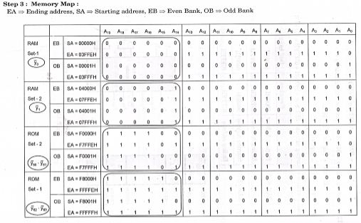
Fig 7 Memory Bank Selection using BHE and BLE Q8) Explain the DRAM interfacing procedure?A8) System design based on memory and peripheralsStep 1: Total EPROM required = 64 KB Chip size available = 16 KB∴Number of chips required=64KB/16KB=4 ∴Number of sets required=Number of chips Number of banks=42=2 SET 1: Ending address of SET 1 = FFFFFH SET size = Chip size x 2 = 16 KB x 2 = 32 KBi.e. 00000011171111F1111F1111F00000011171111F1111F1111F Starting address = Ending address – SET size=FFFFFH–07FFFH SET 2: Ending address of SET 2 = F7FFFH (previous ending - 1) SET size = Chip size x 2 = 16 KB x 2 = 32 KBi.e. 00000011171111F1111F1111F00000011171111F1111F1111F Starting address = Ending address – SET size=F7FFFH–07FFFH=F0000H 
Step 2: Total RAM required = 32 KB Chip size available = 8 KB∴Number of chips required=32KB/8KB=4∴Number of sets required=Number of chips Number of banks=42=2 SET 1: Starting address = 00000H SET size = Chip size x 2 = 8 KB x 2 = 32 KBi.e. 00000001131111F1111F1111F00000001131111F1111F1111FEnding address = Starting address – SET size=04000H+03FFFH=07FFFH SET 2: Starting address = 04000H (previous ending - 1) SET size = Chip size x 2 = 8 KB x 2 = 32 KBi.e. 00000001131111F1111F1111F00000001131111F1111F1111F Ending address = Starting address – SET size=04000H–03FFFH=07FFFH 
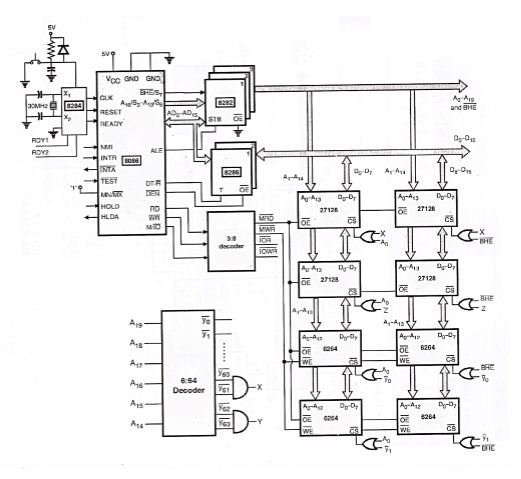
Step 4: Final Implementation:
Fig 8 Final Implementation after interfacing Q9) Explain the I/O interfacing with 8086?A9) Some microprocessors use the same address space for both memory and input/output devices. In this arrangement all instructions that are capable of accessing the memory locations can also access the input/output devices. However, 8086-microprocessor permit the establishment of two separate address spaces for memory and input/output devices. Having separate address space for the input/output devices is called direct I/O. Whenever the 8086 executes an IN and OUT instruction to access a port, none of the segment registers are involved in producing the physical address sent out by the 8086. The port address is sent out directly from the 8086 on lines AD0- AD15, and 0’s is output on lines A16-A19. In an 8086 system which uses direct I/O, the M/IO (Active Low) signal is used to enable a memory decoder or a port decoder. You please remember that the M/IO (Active Low) signal being high was one of the enabling conditions for the memory decoding as we discussed previously. The opposite of this enables the port decoder. During the execution of an IN instruction, the RD (Active Low) signal from the 8086 will be low. This signal can be used to enable an addressed input port device. During the execution of an OUT instruction the WR (Active Low) signal from the 8086 will be low. This signal can be used to enable an output port device. Since the 8086 microprocessor outputs up to 16-bit address for direct I/O operations, it can address any one of the 65536 input ports and any one of the 65536 output ports. However, to achieve this direct I/O, the 8086-microprocessor should be provided with the appropriated decoding circuitry Q10) Explain I/O port addressing?A10) I/0 port address decoding is very similar to memory address decoding, especially for memory mapped 1/0 devices. In fact, we do not discuss memory-mapped I/0 decoding because it is treated exactly the same as memory, except that the  and
and  are not used, since there is no IN or OUT instruction. The decision to use memory-mapped I/0 is often determined by the size of the memory system and the placement of the I/0 devices in the system. The main difference between memory decoding and isolated I/0 decoding is the number of address pins connected to the decoder. We decode A 32-A0, A23-A0, or A 19-A0 for memory and A 15-A0 for isolated I/0. Sometimes, if the I/0 devices use only fixed I/0 addressing, we decode only A7-A0. Another difference is that we use the
  and
and  to activate I/0 devices for a read or a write operation. On earlier versions of the microprocessor, I0/
 = 1 and
  or
or  are used to activate I/0 devices. On the newest versions of the microprocessor, the M/
 = 0 and
  are used to activate I/0 devices.Decoding 8-Bit 1/0 Addresses As mentioned, the fixed I/0 instruction uses an 8-bit l/0 port address that appears on A 15-A0 as OOOOH-OOFFH. If a system will never contain more than 256 I/0 devices, we often decode only address connections A7-A0 for an 8-bit 1/0 port address. Thus, we ignore address connections A 15-A8. Please note that the DX register can also address I/0 ports OOH-FFH. Also note that if the address is decoded as an 8-bit address, then we can never include 1/0 devices that use a 16-bit l/0 address. The 74ALS138 decoder that decodes 8-bit 1/0 ports FOH-F7H. (We assume that the system will only use I/0 ports OOH-FFH for this decoder.) This decoder is identical to a memory address decoder except we only connect address bits A7 -A0 to the inputs of the address lines (A15-A8) must be decoded.
Fig 9 Decoder that generates I/O port address of F0H-F7H
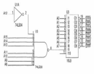
Fig 10 Decoder that Decodes EFF8H-EFFFHFigure above a circuit that contains a PAL16L8 and an 8-input NAND gate used to decode I/0 ports EFF8H-EFFFH. These are common I/0 port assignments in a PC used for the serial communications port. The NAND gate decodes the first 8-bits of the I/0 port address (A 15-A8) so that it generates a signal to enable the PAL16L8 for any I/0 address between EFOOH and EFFFH.
|
|
|
|
|
|
|


|
|
 and
and  are not used, since there is no IN or OUT instruction. The decision to use memory-mapped I/0 is often determined by the size of the memory system and the placement of the I/0 devices in the system. The main difference between memory decoding and isolated I/0 decoding is the number of address pins connected to the decoder. We decode A 32-A0, A23-A0, or A 19-A0 for memory and A 15-A0 for isolated I/0. Sometimes, if the I/0 devices use only fixed I/0 addressing, we decode only A7-A0. Another difference is that we use the
  and
and  to activate I/0 devices for a read or a write operation. On earlier versions of the microprocessor, I0/
 = 1 and
  or
or  are used to activate I/0 devices. On the newest versions of the microprocessor, the M/
 = 0 and
  are used to activate I/0 devices.Decoding 8-Bit 1/0 Addresses As mentioned, the fixed I/0 instruction uses an 8-bit l/0 port address that appears on A 15-A0 as OOOOH-OOFFH. If a system will never contain more than 256 I/0 devices, we often decode only address connections A7-A0 for an 8-bit 1/0 port address. Thus, we ignore address connections A 15-A8. Please note that the DX register can also address I/0 ports OOH-FFH. Also note that if the address is decoded as an 8-bit address, then we can never include 1/0 devices that use a 16-bit l/0 address. The 74ALS138 decoder that decodes 8-bit 1/0 ports FOH-F7H. (We assume that the system will only use I/0 ports OOH-FFH for this decoder.) This decoder is identical to a memory address decoder except we only connect address bits A7 -A0 to the inputs of the address lines (A15-A8) must be decoded.
|
|
0 matching results found

