MICRO
UNIT 8I/O Interface – 2, Interrupts, and DMA Q1) Explain BSR mode of 8255?A1) The Bit Set/Reset (BSR) mode is available on port C only. Each and every line of port C (PC7 - PC0) can be set or reset by providing a suitable value to the control word register. BSR mode is independent and its selection does not affect the operation of other ports in I/O mode.
D7 bit is always 0 for this mode. Bits D6, D5 and D4 are don't care bits. Bits D3, D2 and D1 are used for pin selection of Port C. Bit D0 is used to set/reset the above selected pin. Selection of port C pin is determined as follows:
For example:If PC4 be set, then in the control word is, Since it is a BSR mode, D7 = '0'. Since D4, D5, D6 are don’t care hence assuming them to be '0'. PC4 has to be selected, hence, D3 = '1', D2 = '0', D1 = '0'. PC4 has to be set, hence, D0 = '1'. Thus, as per the above values, 0AH (in hex) will be loaded into the Control Word Register (CWR). Q2) Explain the operating modes of 8253?A2) 8253 can be operated in 6 different modes. They are:Mode 0 ─ Interrupt on Terminal Count It is used for generating an interrupt to the microprocessor after a certain interval. The output is low after the mode is set and remains LOW after the count value is loaded into the counter. The counter decrement continues till the terminal count is reached. The GATE signal remains high for normal counting. When it is low, counting is terminated and the current count is latched till it goes high again. Mode 1 – Programmable One Shot It is used as a mono stable multi-vibrator. GATE is used as a trigger input in this mode. As the count is loaded the output remains high and a trigger is applied. Mode 2 – Rate Generator The output is high after initialization. Whenever the count becomes zero, a low pulse is generated at the output and the counter is reloaded. Mode 3 – Square Wave Generator This mode is same as Mode 2 except that the output remains low for half of the timer period and high for the next half of the period. Mode 4 − Software Triggered Mode In this, the output remains high till the timer counts to zero and at this point the output is low and then goes high again. The count is latched when GATE LOW. As per the terminal count, for one clock cycle the output goes low then goes HIGH. The low pulse is used as a strobe. Mode 5 – Hardware Triggered Mode This mode generates a strobe as a result to an externally generated signal. It is same as mode 4 except that the counting is initiated by a signal at the gate input. As soon as it is initialized, the output goes high. When the terminal count is reached, the output goes low for one clock cycle. Q3) Explain the control word register of 8253/8254?A3) This register can be accessed when lines A0 & A1 are at logic 1. It is used to write a command word, its mode and either a read or write operation. Following table provides the result for various control inputs:
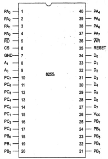
Q4) Explain pin diagram of 8255?A4)
Fig.1: Pin Configuration of 8255It is also known as Programmable Peripheral Interface. It is a multi port device. It has 24 I/O pins. They are divided into three 8 bit ports PA, PB, PC. Port A and port B are used as 8-bit I/O ports. Port C is used as an 8-bit I/O port or as two 4-bit I/O ports or produces handshake signals for ports A and B. CS: The chip select CS (pin 6) is used to enable the 8255 chip. It is an active-low signal, hence is enabled when CS = 0. RESET: It is an input pin 35 and is connected to the RESET line of system 8085. When the system is reset, all the ports behave as input lines. This is done to prevent 8255 from being destroyed due to mismatch of ports. Eight data lines (D0–D7) are available to read/write data into the ports or control register under the status of the RD (pin 5) and WR (pin 36), which are active-low signals for read and write operations respectively. Address lines A1 and A0 allow to access a data register for each port or a control register, as listed below:
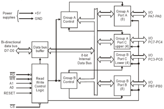
Q5) Explain IO modes of 8255?A5) I/O MODEWhen D7 bit of the Control Word Register is 1, this mode is selected. There are three I/O modes and they are: Mode 0 - Simple I/O Mode 1 - Strobed I/O Mode 2 - Strobed Bi-directional I/O Mode 0 – Simple or basic I/O mode: Port A, B and C can work either as input or as output function. The outputs are latched but the inputs are not latched. It can handle interrupts.Mode 1 – Handshake or strobbed I/O: Here, either port A or B can work and port C is used to provide handshake signals. The outputs as well as inputs are latched. It can handle interrupts. Before actual data is transmitted, there is transmission of signal to match speed of CPU and printer. Mode 2 – Bidirectional I/O: In this mode only port A will work, port B can either is in mode 0 or 1 and port C bits are used as handshake signal. The outputs as well as inputs are latched. It has interrupt handling capability. Q6) Explain the functional block diagram of 8255?A6) Functional block diagram
Fig 2 Functional Block Diagram Control Word for I/O mode
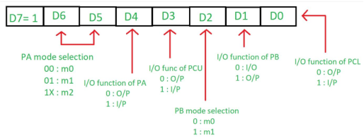
The most significant bit (D7) is 1 for the I/O mode. D6 & D5: It is used to set the port A mode.
D4 : It is used to check whether port A is taking input or displaying the output. If it is 1 then input else output. D3: It is used to check whether port C higher bites takes input or output. If 1, then input else output. D2: It tells the mode of port B. If 0, then port B is in M0 mode else in M1 mode. D1: It is used to check whether port B is taking input or displaying output. If 1, then input else output. D0: It is used to tell whether port C lower bits is taking input or displaying output. If 1, then it takes input else displays output. Q7) Explain operating modes of 8253?A7)
|
D3 | D2 | D1 | Bit/pin of port C selected |
0 | 0 | 0 | PC0 |
0 | 0 | 1 | PC1 |
0 | 1 | 0 | PC2 |
0 | 1 | 1 | PC3 |
1 | 0 | 0 | PC4 |
1 | 0 | 1 | PC5 |
1 | 1 | 0 | PC6 |
1 | 1 | 1 | PC7 |
A1 | A0 | RD | WR | CS | Result |
0 | 0 | 1 | 0 | 0 | Write Counter 0 |
0 | 1 | 1 | 0 | 0 | Write Counter 1 |
1 | 0 | 1 | 0 | 0 | Write Counter 2 |
1 | 1 | 1 | 0 | 0 | Write Control Word |
0 | 0 | 0 | 1 | 0 | Read Counter 0 |
0 | 1 | 0 | 1 | 0 | Read Counter 1 |
1 | 0 | 0 | 1 | 0 | Read Counter 2 |
1 | 1 | 0 | 1 | 0 | No operation |
X | X | 1 | 1 | 0 | No operation |
X | X | X | X | 1 | No operation |
|
A1 | A0 | PORT SELECTED |
0 | 0 | PORT A |
0 | 1 | PORT B |
1 | 0 | PORT C |
1 | 1 | Control Register |
|
|
|
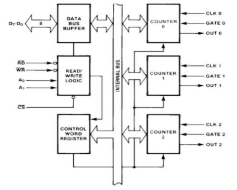
8253 can be operated in 6 different modes. They are:Mode 0 ─ Interrupt on Terminal Count It is used for generating an interrupt to the microprocessor after a certain interval. The output is low after the mode is set and remains LOW after the count value is loaded into the counter. The counter decrement continues till the terminal count is reached. The GATE signal remains high for normal counting. When it is low, counting is terminated and the current count is latched till it goes high again. Mode 1 – Programmable One Shot It is used as a mono stable multi-vibrator. GATE is used as a trigger input in this mode. As the count is loaded the output remains high and a trigger is applied. Mode 2 – Rate Generator The output is high after initialization. Whenever the count becomes zero, a low pulse is generated at the output and the counter is reloaded. Mode 3 – Square Wave Generator This mode is same as Mode 2 except that the output remains low for half of the timer period and high for the next half of the period. Mode 4 − Software Triggered Mode In this, the output remains high till the timer counts to zero and at this point the output is low and then goes high again. The count is latched when GATE LOW. As per the terminal count, for one clock cycle the output goes low then goes HIGH. The low pulse is used as a strobe. Mode 5 – Hardware Triggered Mode This mode generates a strobe as a result to an externally generated signal. It is same as mode 4 except that the counting is initiated by a signal at the gate input. As soon as it is initialized, the output goes high. When the terminal count is reached, the output goes low for one clock cycle. Q8) Explain the functional block diagram of 8253?A8) Functional block diagram:
Fig 3 Block Diagram of 8253 Control Word Register
|
This register can be accessed when lines A0 & A1 are at logic 1. It is used to write a command word, its mode and either a read or write operation. Following table provides the result for various control inputs:
Q9) Explain the dedicated interrupts?A9) Dedicated interrupts (INT 0…..INT 4):INT 0 (Divide Error)- INT 1 (Single Step)- INT 2 (Non mask-able Interrupt)- INT 3 (Breakpoint Interrupt)- INT 4 (Overflow Interrupt)- Q10) Mention the hardware interrupts of 8086?A10) Hardware Interrupts:NMI (Non mask-able interrupt)- INTR- This is a mask-able, level triggered, low priority interrupt. On receiving an interrupt on INTR line, the microprocessor executes 2 INTA pulses. It is masked by making IF = 0 by software through CLI instruction. It is unmasked by making IF = 1 by software through STI instruction.
A1 | A0 | RD | WR | CS | Result |
0 | 0 | 1 | 0 | 0 | Write Counter 0 |
0 | 1 | 1 | 0 | 0 | Write Counter 1 |
1 | 0 | 1 | 0 | 0 | Write Counter 2 |
1 | 1 | 1 | 0 | 0 | Write Control Word |
0 | 0 | 0 | 1 | 0 | Read Counter 0 |
0 | 1 | 0 | 1 | 0 | Read Counter 1 |
1 | 0 | 0 | 1 | 0 | Read Counter 2 |
1 | 1 | 0 | 1 | 0 | No operation |
X | X | 1 | 1 | 0 | No operation |
X | X | X | X | 1 | No operation |
- This interrupt occurs whenever there is division error. This condition normally occurs when the divisor is very small as compared to the dividend or the divisor is zero.
- Its ISR address is stored at location 0 x 4 = 00000H in the IVT.
- The microprocessor executes this interrupt after every instruction if the TF is set.
- Its ISR displays contents for all registers. Its ISR address is stored at location 1 x 4 = 00004H in the IVT.
- The microprocessor executes this ISR in response to an interrupt on the NMI (Non mask-able Interrupt) line.
- Its ISR address is stored at location 2 x 4 = 00008H in the IVT.
- This interrupt causes breakpoints in the program. It occurs by writing the instruction INT 03H or simply INT.
- It is useful in debugging large programs.
- Its ISR is used to display the contents of all registers on the screen. Its ISR address is stored at location 3 x 4 = 0000CH in the IVT.
- It occurs if the overflow flag is set and the microprocessor executes the INTO (Interrupt on Overflow) instruction.
- It detects overflow error in signed arithmetic operations.
- Its ISR address is stored at location 4 x 4 = 00010H in the IVT.
- This is a non-mask-able, edge triggered, high priority interrupt.
- On receiving this, the microprocessor executes INT instruction.
- Microprocessor obtains the ISR address from location 2 x 4 = 00008H from the IVT.
- It reads 4 locations starting from this address to get the values for IP and CS to execute the ISR.
0 matching results found


