 A1)
A1)
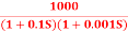
G(j This is type 0 system. so initial slope is 0 dB decade. The starting point is given as 20 log10 K = 20 log10 1000= 60 dB Corner frequency
Slope after
|


3. |


 100 -900200 -9.450300 -104.80400 -110.360500 -115.420600 -120.00700 -124.170800 -127.940900 -131.3501000 -134.420The plot is shown in figure 1:
|
|
 Q2) For the given transfer function determine G(S) =
  A2) Gain cross over frequency phase cross over frequency phase mergence and gain margin
Initial slope = 1 N = 1, (K)1/N = 2 K = 2 Corner frequency
2. phase
1 -119.430 5 -172.230 10 -195.250 15 -209.270 20 -219.30 25 -226.760 30 -232.490 35 -236.980 40 -240.570 45 -243.490 50 -245.910 Finding M = 4 =
Let X3 (6.25 X1 = 2.46 X2 = -399.9 X3 = -6.50 For x1 = 2.46
for phase margin PM = 1800 -
= -164.50 PM = 1800 - 164.50 = 15.50 For phase cross over frequency (
-1800 = -900 – tan-1 (0.5 -900 – tan-1 (0.5 Taking than on both sides Tan 900 = tan-1 Let tan-1 0.5
1 =0.5
|


|
|
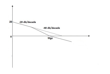
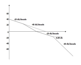
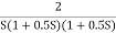 Q3) For the given transfer function G(S) =
 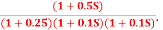 Plot the rode plot find PM and GMA3) T1 = 0.5
  1 =
1 =  = 2 rad/secZero so, slope (20 dB/decade)T2 = 0.2
  2 =
2 =  = 5 rad/secPole, so slope (-20 dB/decade)T3 = 0.1 = T4 = 0.1
 3 =
3 =  4 = 10 (2 pole ) (-40 dB/decade)
 1 = 2 rad/sec
 1 to
1 to 2 (i.e. 2 rad /sec to 5 rad/sec) slope will be 20 dB/decade
 2 to
2 to  3 the slope will be 0 dB/decade (20 + (-20))
 3 ,
3 , 4 the slope will be -40 dB/decade (0-20-20)
 = tan-1 0.5
 - tan-1 0.2
 - tan-1 0.1
 - tan-1 0.1

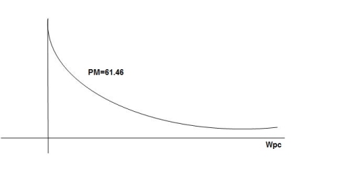
 500 -177.301000 -178.601500 -179.102000 -179.402500 -179.503000 -179.5303500 -179.60GM = 00PM = 61.460The plot is shown in figure 3
|
|
|
|
|
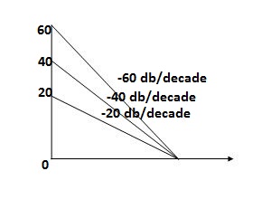
 Q4) For the given transfer function plot the bode plot (magnitude plot) G(S)=
 A4) Given transfer functionG(S) =
  Converting above transfer function to standard fromG(S) =
  =
= 
 ,
,  11= 5 (zero)T2 = 1 ,
  2 = 1 (pole)4. Initial slope will cut zero dB axis at (K)1/N = 10i.e.
  = 105. finding
  n and
n and  T(S) =
  T(S)=
T(S)=  Comparing with standard second order system equationS2+2
 ns +
ns + n2
n2 n = 11 rad/sec
 n = 5
n = 5 11 = 5
 =
=  = 0.276. Maximum errorM = -20 log 2
 = +6.5 dB7. As K = 10, so whole plot will shift by 20 log 10 10 = 20 dBThe plot is shown in figure 4
|
|
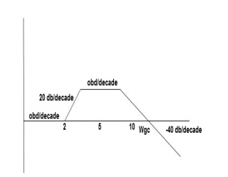
 Q5) For the given plot determine the transfer function
|
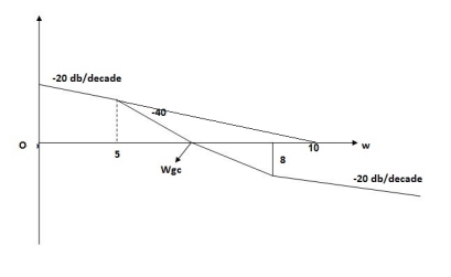
 = 10 so
  1 =
1 =  = 0.2 rad/sec
 2 =
2 =  = 0.125 rad/sec4. At
  = 5 the slope becomes -40 dB/decade, so there is a pole at
  = 5 as
  = 8 the slope changes from -40 dB/decade to -20 dB/decade hence
  = 8 (-40+(+20) = 20)
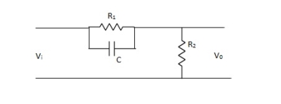
 Q6) Draw and explain phase lead compensator?A6) The phase of output voltage leads the phase of input voltage for the applied sinusoidal input. The circuit diagram is shown below. The transfer function is given as,
|
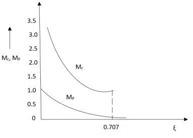
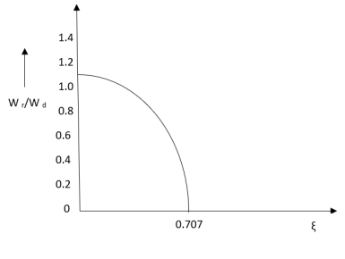
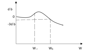
C(S)/R(S) = W2n / S2 + 2ξWnS + W2n - - (1) ξ = Ramping factor Wn = Undamped natural frequency for frequency response let S = jw C(jw) / R(jw) = W2n / (jw)2 + 2 ξWn(jw) + W2n Let U = W/Wn above equation becomes T(jw) = W2n / 1 – U2 + j2 ξU so, | T(jw) | = M = 1/√ (1 – u2)2 + (2ξU)2 - - (2) T(jw) = φ = -tan-1[ 2ξu/(1-u2)] - - (3) For sinusoidal input the output response for the system is given by C(t) = 1/√(1-u2)2 + (2ξu)2Sin [wt - tan-1 2ξu/1-u2] - - (4) The frequency where M has the peak value is known as Resonant frequency Wn. This frequency is given as (from eqn (2)). dM/du|u=ur = Wr = Wn√(1-2ξ2) - - (5) from equation (2) the maximum value of magnitude is known as Resonant peak. Mr = 1/2ξ√1-ξ2 - - (6) The phase angle at resonant frequency is given as Φr = - tan-1 [√1-2ξ2/ ξ] - - (7) |
|
|
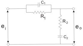
 T2)Where, αT1 = R1C1
  T2= R2C2we can say in the lag-lead compensation pole is more dominating than the zero and because of this lag-lead network may introduces positive phase angle to the system when connected in series. Q9) List difference between phase lead and phase lag compensator?A9)
Phase Lead Network Phase Lag Network 1>. It is used to improve the 1>It is used to improve the transient response. Steady state response. 2>. It acts as a high pass filter. 2>It acts as a low pass filter. 3>. The system becomes fast as 3>The Bandwidth decreases Bandwidth increases as rise through rise time the speed Time decreases. is slow. 4>. As the circuit acts as 4>Signal to noise ratio is higher as it a differentiator, signal to acts as integrator. noise ratio is poor. 5>. Maximum peak overshoot 5>It reduces steady state error thus is reduced. improve the steady state accuracy
|
|
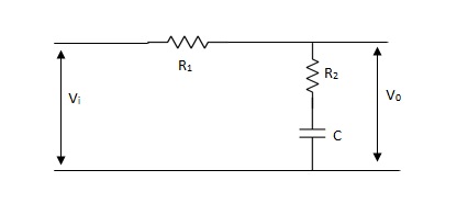
Vo/Vi = 1 + ST/1 + SβT Where, β = R1 + R2/R2, β> 1 T = R2C w = 1/T upper corner frequency due to zero w= 1/βT lower corner frequency due to pole The mid frequency wm, wm = 1/T√β The maximum phase lead angle Φm Φm = tan-11- β/2 √β = sin-11 – β/1 + β |


