LICA
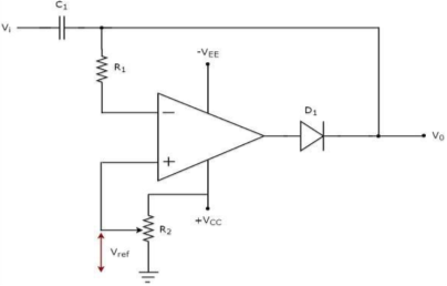
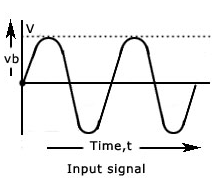
UNIT-5More ApplicationsQ1) Explain positive clamper circuit with the output waveforms?A1) A clamper is an electronic circuit that produces an output, which is similar to the input but with a shift in the DC level. In other words, the output of a clamper is an exact replica of the input. Hence, the peak to peak amplitude of the output of a clamper will be always equal to that of the input.Positive ClamperA positive clamper is a clamper circuit that produces an output in such a way that the input signal gets shifted vertically by a positive DC value.The circuit diagram of a positive clamper is shown in the following figure
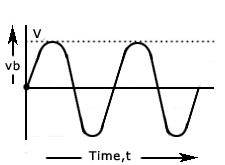
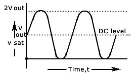
Fig 1 Positive Clamper CircuitIn the above circuit, a sinusoidal voltage signal, Vi is applied to the inverting terminal of op-amp through a network that consists of a capacitor C1 and a resistor R1. That means, AC voltage signal is applied to the inverting terminal of the op-amp.The DC reference voltage Vref is applied to the non-inverting terminal of the op-amp. The value of reference voltage Vref can be chosen by varying the resistor R2. In this case, we will get a reference voltage Vref of a positive value.The above circuit produces an output, which is the combination of the sinusoidal voltage signal Vi and the reference voltage Vref. That means, the clamper circuit produces an output in such a way that the sinusoidal voltage signal Vi gets shifted vertically upwards by the value of reference voltage Vref.The input wave form and the corresponding output wave form of positive clamper are shown in above figure
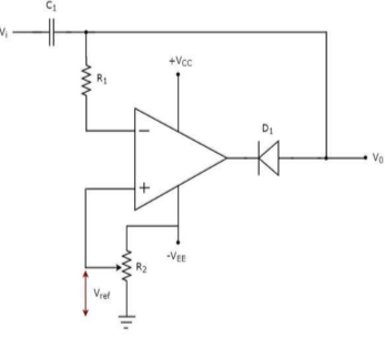
Fig 2 Input and Output waveform of positive clamper Q2) Explain Negative clamper circuits?A2) A negative clamper is a clamper circuit that produces an output in such a way that the input signal gets shifted vertically by a negative DC value.
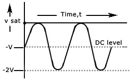
Fig 3 Negative ClamperIn the above circuit, a sinusoidal voltage signal Vi is applied to the inverting terminal of the op-amp through a network that consists of a capacitor C1 and resistor R1. That means, AC voltage signal is applied to the inverting terminal of the op-amp.The DC reference voltage Vref is applied to the non-inverting terminal of the op-amp. The value of reference voltage Vref can be chosen by varying the resistor R2. In this case, we will get reference voltage Vref of a negative value.The above circuit produces an output, which is the combination of sinusoidal voltage signal Vi and reference voltage Vref. That means, the clamper circuit produces an output in such a way that the sinusoidal voltage signal Vi gets shifted vertically downwards by the value of reference voltage Vref.
Fig 4 Input and Output waveform of Negative Clamper Q3) Explain peak detector circuit?A3)
|
|
|
|
|
|
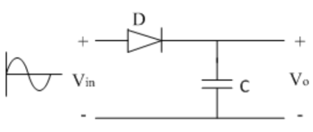
Rectifier circuit gives average value of input signal; but in practice we need peak value of input signal. This is achieved by peak detector circuit. The following figure shows a simple peak detector circuit using diode and capacitor.
Fig 5 Peak detectorIn the positive half cycle, diode D is forward biased and capacitor C starts charging. When input reaches its peak value, capacitor gets charged to positive peak value.
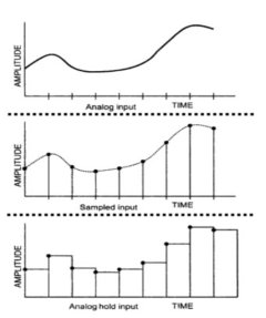
In negative half cycle, as input decreases, diode D is reversed biased and capacitor is isolated and holds the peak value of previous cycle. Hence called as peak detector.But in practice, output is taken across some load RL, so when input voltage decreases capacitor discharges through load RL. To avoid this, select RL of very large value so that capacitor discharges very slowly hence almost hold the charge. Whatever charge it lost through RL is gets back in next half cycle. Q4) Explain sample and hold circuit and its need?A4)The Sample and Hold circuit is an electronic circuit which creates the samples of voltage given to it as input, and after that, it holds these samples for the definite time. The time during which sample and hold circuit generates the sample of the input signal is called sampling time. Similarly, the time duration of the circuit during which it holds the sampled value is called holding time. Sampling time is generally between 1µs to 14 µs while the holding time can assume any value as required in the application. It will not be wrong to say that capacitor is the heart of sample and hold circuit. This is because the capacitor present in it charges to its peak value when the switch is opened, i.e during sampling and holds the sampled voltage when the switch is closed. Need for Sample and Hold CircuitsIf the input analog voltage of an ADC changes more than ±1/2 LSB, then there is a severe chance that the output digital value is an error. For the ADC to produce accurate results, the input analog voltage should be held constant for the duration of the conversion.It is based on a sampling command and holds the output value at its output until the next sampling command is arrived.The following image shows the input and output of a typical Sample and Hold Circuit.
Fig 6 Input and output of S/H circuitThis sample and hold circuit consist of two basic components:Analog Switch Holding Capacitor
Q5) Explain the specifications based on S/H circuit characteristics?A5)
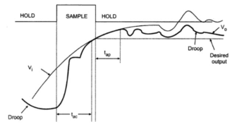
Fig 9 S/H characteristicsAcquisition Time (tac)The time required for the charge in the holding capacitor to rise up to a level that is close to the input voltage during the sampling is called acquisition time. It is affected by three factors:The RC Time Constant The Slew-Rate of the Op-Amp The maximum output current of the Op-Amp Aperture Time (tap)The time delay between the initiation of VO tracking the Vi and the initiation of the hold command is called the Aperture Time. This delay is usually due to the propagation delays through the driver and the switch circuits.For a precise timing operation, the hold command must be initiated in advance by an amount of aperture time.Aperture Uncertainty (∆ tap)The Aperture time will not be the same for all the sample and will vary from sample to sample. This uncertainty is called Aperture Uncertainty. This will severely affect the advancing of the hold command.Hold Mode Settling Time (ts)The hold mode settling time is the time taken by the output VO to settle within the specified error band (usually 1%, 0.1% or 0.01%) after the application of hold command.Hold StepDuring the switching from sample mode to hold mode, there might an unwanted transfer of charge between the switch and the holding capacitor (mainly due to the parasitic capacitances). This will affect the capacitor voltage as well as the output voltage. This change in the output voltage from the desired voltage is called Hold Step.FeedthroughAgain, the parasitic capacitances in the switch may cause AC coupling between VO and Vi in hold mode. As a result, the output voltage may vary with changes in the input voltage and this is referred to as feedthrough.DroopVoltage Droop is a phenomenon where the voltage across the holding capacitor drops down due to leakage currents. Q6) What are V-I converters? A6) A voltage to current converter or V to I converter, is an electronic circuit that takes current as the input and produces voltage as the output. An op-amp based voltage to current converter produces an output current when a voltage is applied to its non-inverting terminal. The circuit diagram of an op-amp based voltage to current converter is shown in the following figure.
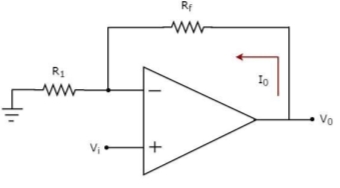
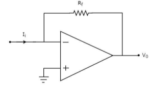
Fig 10 V-I ConverterIn the circuit shown above, an input voltage Vi is applied at the non-inverting input terminal of the op-amp. According to the virtual short concept, the voltage at the inverting input terminal of an op-amp will be equal to the voltage at its non-inverting input terminal. So, the voltage at the inverting input terminal of the op-amp will be Vi.The nodal equation at the inverting input terminal's node is −ViR1−I0=0=>I0=VtR1Thus, the output current I0 of a voltage to current converter is the ratio of its input voltage Vi and resistance R1.We can re-write the above equation as −I0/Vi=1/R1The above equation represents the ratio of the output current I0 and the input voltage Vi & it is equal to the reciprocal of resistance R1. The ratio of the output current I0 and the input voltage Vi is called as Transconductance. Q7) What are I-V converters?A7) A current to voltage converter or I to V converter is an electronic circuit that takes current as the input and produces voltage as the output. An op-amp based current to voltage converter produces an output voltage when current is applied to its inverting terminal. The circuit diagram of an op-amp based current to voltage converter is shown in the following figure.
Fig 11 I-V ConverterIn the circuit shown above, the non-inverting input terminal of the op-amp is connected to ground. That means zero volts is applied at its non-inverting input terminal.According to the virtual short concept, the voltage at the inverting input terminal of an op-amp will be equal to the voltage at its non-inverting input terminal. So, the voltage at the inverting input terminal of the op-amp will be zero volts.The nodal equation at the inverting terminal's node is −−Ii+0−V0/Rf=0−Ii=V0/RfV0=−Rf.IiThus, the output voltage, V0 of current to voltage converter is the (negative) product of the feedback resistance, Rf and the input current, It. Observe that the output voltage, V0 is having a negative sign, which indicates that there exists a 1800 phase difference between the input current and output voltage.We can re-write the above equation as −V0/Ii=−RfThe above equation represents the ratio of the output voltage V0 and the input current Ii, and it is equal to the negative of feedback resistance, Rf. The ratio of output voltage V0 and input current Ii is called as Trans-resistance. Q8) Explain Log amplifiers using op-amps and also derive the output equations?
|
In negative half cycle, as input decreases, diode D is reversed biased and capacitor is isolated and holds the peak value of previous cycle. Hence called as peak detector.But in practice, output is taken across some load RL, so when input voltage decreases capacitor discharges through load RL. To avoid this, select RL of very large value so that capacitor discharges very slowly hence almost hold the charge. Whatever charge it lost through RL is gets back in next half cycle. Q4) Explain sample and hold circuit and its need?A4)
|
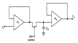
Fig 7 Open loop s/h circuit
|
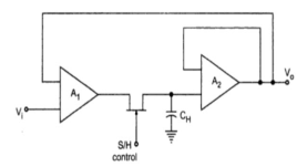
Fig 8 Closed loop s/h circuit
|
|
|
|
A8) As the name says it is an amplifier which produces the output proportional to logarithmic of the applied input. The log amplifier using op-amp is shown below. The input is applied through the inverting end of op-amp. As the non-inverting end has voltage zero then by virtual ground concept the voltage at inverting terminal also becomes zero.
Fig 12 Log Amplifier
The above equations shows that the output is natural log of the applied input. Q9) Explain antilog amplifiers with the output equation?A9)
|
The equation for input voltage will be
If = The current flowing through diode is given as
Where: Is = Saturation Current Vf = Voltage drop across diode in forward bias VT = Thermal equivalent voltage For feedback loop the KVL equation will be 0-Vf -V0 = 0 Vf = -V0 Substituting Vf in above equation of If
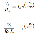
Equating both equations of If
Taking natural log of both sides we get
|
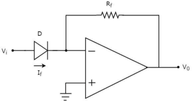
This device produces the output proportional to antilog of input. The inverting op-amp is used in this case as well. The figure below shows an antilog amplifier with its inverting terminal connected to the input end with diode and the non-inverting terminal is grounded.
Fig 13 Antilog Amplifier
Q10) Explain square wave generator?A10) The square wave generator is based on a uA741 opamp (IC1). Resistor R1 and capacitor C1 determines the frequency of the square wave. Resistor R2 and R3 forms a voltage divider setup which feedbacks a fixed fraction of the output to the non-inverting input of the IC.Initially, when power is not applied the voltage across the capacitor C1 is 0. When the power supply is switched ON, the C1 starts charging through the resistor R1 and the output of the op-amp will be high. A fraction of this high voltage is fed back to the non- inverting pin by the resistor network R2, R3. When the voltage across the charging capacitor is increased to a point the voltage at the inverting pin is higher than the non-inverting pin, the output of the op-amp swings to negative saturation (-Vcc). The capacitor quickly discharges through R1 and starts charging in the negative direction again through R1. Fraction of the negative high output (-Vcc) is fed back to the non-inverting pin by the feedback network R2, R3. When the voltage across the capacitor has become so negative that the voltage at the inverting pin is less than the voltage at the non-inverting pin, the output of the op-amp swings back to the positive saturation. Now the capacitor discharges trough R1 and starts charging in positive direction. This cycle is repeated over time and the result is a square wave swinging between +Vcc and -Vcc at the output of the op-amp. If the values of R2 and R3 are made equal, then the frequency of the square wave can be expressed using the following equationF = 1/(2.1976 R1C1)
|
Applying KCL at input terminal we get
The current flowing through diode is given as
Substituting If in above voltage equation we get
At inverting terminal applying KVL we get
Substituting Vf in equation of V0 we get
The above equations shows that the output is natural antilog of the applied input.
|
0 matching results found
