Back to Study material
LICA

UNIT-8Other Linear IC ApplicationsQ1) Explain block diagram of 555 timers?A1)

Fig 1 IC 555 TimerFor IC555 timer working as a flip flop or as a multi-vibrator, it has a particular set of configurations. Some of the major features include:
  • It operates from a wide range of power ranging from +5 Volts to +18 Volts supply voltage.
  • Sinking or sourcing 200 mA of load current.
  • The external components should be selected properly so that the timing intervals can be made into several minutes along with the frequencies exceeding several hundred kilohertz.
  • The output of a 555 timer can drive a transistor-transistor logic (TTL) due to its high current output.
  • It has a temperature stability of 50 parts per million (ppm) per degree Celsius change in temperature which is equivalent to 0.005 %/ °C.
  • The duty cycle of the timer is adjustable.
  • Also, the maximum power dissipation per package is 600 mW and its trigger and reset inputs has logic compatibility.
  •  Q2) Explain astable multivibrator?A2)

    This means there will be no stable level at the output. So, the output will be swinging between high and low. This character of unstable output is used as a clock or square wave output for many applications.

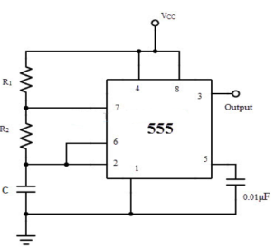
    Fig 2 Astable MultivibratorIt is self-triggered multivibrator as pin 2 and 6 are connected. The supply is given through pin 8 and the output is obtained through pin 3. The timer will be reset if a low signal is given to pin 4. The capacitor is connected across pin 5 so that the external noise or any dc level are filtered. The resistor pair R1 and R2 form a circuit for determining the width of the output pulse.

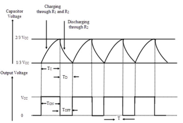
    Fig 3 Capacitor and Output voltage waveformDuring charging the capacitor charges through R1 and R2 and voltage across capacitor rises exponentially and during discharging the capacitor discharges through R2 and voltage falls exponentially. The output is obtained across pin 3.

    The time for which capacitor charges from 1/3VCC to 2/3VCC is equal to the time the output is high which is given by

    tc= 0.69(R1+R2) C

    The discharging time from 2/3Vcc to 1/3VCC is given as

    td= 0.69 R2C

    The total period of output waveform is given by

    T = tc+ td = 0.69(R1+2R2) C

    The frequency of oscillations is given by

    f0 = =

    The duty cycle is defined as the ratio of the charging time of capacitor at which the output is high to the total time period.

    %duty cycle = x 100

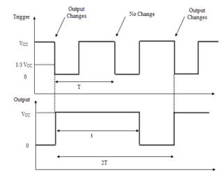
     Q3) Explain frequency divider circuit using monostable multivibrator?A3) The monostable multivibrator can be used as frequency divider by adjusting the time interval off charging. The charging time is made larger than the period of input pulse the device acts as divide-by-2 network. By proper selection of R and C the timing interval can be controlled. The waveform is shown below.

    Fig 3 Divide-by-2 circuit waveformWhen negative input pulse is applied the output goes high and will remain high irrespective of any other input pulse application as the timing interval s greater than the time period of trigger pulse. The circuit is triggered for every alternate negative going pulse. Q4) Draw and explain pulse stretcher circuit?A4) This application makes use of the fact that output pulse width of monostable multivibrator is larger than the negative pulse width of trigger pulse. The output of monostable multivibrator is the stretched form of the input pulse. The pulse stretcher is shown below.

    Fig 4 Pulse StretcherQ5)

    An Astable 555 Oscillator is constructed using the following components, R1 = 1kΩ, R2 = 2kΩ and capacitor C = 10uF. Calculate the output frequency from the 555 oscillator and the duty cycle of the output waveform.A5)

    t1 – capacitor charge “ON” time is calculated as:

    t1 = 0.693(R1 + R2). C

        = 0.693(1000 +2000) x 10 x 10 -6 = 0.021 s= 0.21 msec

    t2 – capacitor discharge “OFF” time is calculated as:

    t2 = 0.693 R2. C

        = 0.693 X 2000 x 10 x 10 -6 = 14ms

    Total periodic time (T) is therefore calculated as:

    T = t1 + t2 = 21 ms + 14 ms = 35 ms.

    The output frequency, ƒ is therefore given as:

     f = 1/T = 1/35ms = 28.6 Hz

    Giving a duty cycle value of:

    Duty Cycle = R1 + R2 / (R1 + 2 R2) = 1000 + 2000/ (1000 + 2 x 2000) = 60%


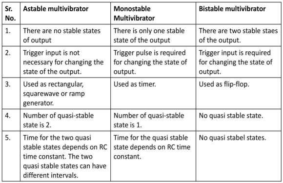
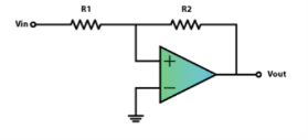
     Q6) Explain and compare the astable, monostable and bistable multivibrators?A6) Q7) Explain Schmitt trigger circuit?A7) The Schmitt Trigger is a logic input type that provides hysteresis or two different threshold voltage levels for rising and falling edge. This is useful because it can avoid the errors when we have noisy input signals from which we want to get square wave signals.SymmetricalIf we add a positive feedback by connecting the output voltage to the non-inverting input with a resistor between them and another resistor between the VIN and the non-inverting input, we will get the Schmitt Trigger. Now the output will switch from VCC– to VCC+ when the voltage at the A node will cross 0 volts.That means that now by adjusting the values of the resistors we can set at what value of the VIN input the switch will occur using the following equations. We get these equations with the following relationships. The current “i” through this line equals VIN – VA divided by R1 as well as VA – VOUT divided by R2. So if we replace the VA with zero, as we need that value for the switch to occur, we will get that final equation.

    Fig 5 Symmetrical

    Va = 0


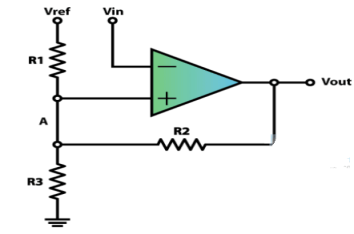
    Fig 6 Symmetrical characteristics Asymmetrical In order to get two different non-symmetrical thresholds, we can use this circuit of an inverting single powered Schmitt Trigger. Here the VREF voltage is the same as the VCC of the op-amp. Now because the VIN input is connected to the inverting input of the op-amp when its values will reach the upper threshold, the output will switch off to 0 volts, and then when its values will decline to the lower threshold, the output will switch on to 5 volts.

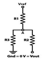
    Fig 7 Asymmetrical Q8) The VREF = VCC = 5 volts and the three resistors will be the same 10k ohms. So, calculate the voltage at the A node.  Assume Vout =0V and 5V.A8)


    Vout = 0V


    Va = 166V

    Vout = 5V

    Va = 333V

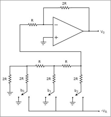
     Q9) Explain R-2R Ladder Circuit?A9) The R-2R Ladder DAC overcomes the disadvantages of a binary weighted resistor DAC. As the name suggests, R-2R Ladder DAC produces an analog output, which is almost equal to the digital (binary) input by using a R-2R ladder network in the inverting adder circuit.The circuit diagram of a 3-bit R-2R Ladder DAC is shown in the following figure

    Ladder DAC

    Fig 8 R-2R LadderLet the 3-bit binary input is b2b1b0. Here, the bits b2 and b0 denote the Most Significant Bit (MSB) and Least Significant Bit (LSB) respectively.The digital switches shown in the above figure will be connected to ground, when the corresponding input bits are equal to ‘0’. Similarly, the digital switches shown in above figure will be connected to the negative reference voltage, VR when the corresponding input bits are equal to ‘1’.It is difficult to get the generalized output voltage equation of a R-2R Ladder DAC. But, we can find the analog output voltage values of R-2R Ladder DAC for individual binary input combinations easily.The advantages of a R-2R Ladder DAC are as follows
  •     R-2R Ladder DAC contains only two values of resistor: R and 2R. So, it is easy to select and design more accurate resistors.
  •     If more number of bits are present in the digital input, then we have to include required number of R-2R sections additionally.
  •  Q10) Explain Dual Slope ADC?A10)

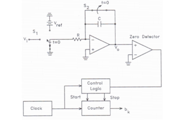
    Fig 9 Dual Slope ADC Working: 
  • At t<0, S1 is set to ground, S2 is closed and counter =0.
  • At t=0 conversion begins and S2 is open and S1 is set so the input to the integrator is Vin.
  • Si is held for T INT   which is a constant predetermined time interval.
  • When S1 is set the counter begins to count clock pulses, the counter resets to zero after TINT
  • Vout of integrator at t=TINT is Vin TINT /RC linearly proportional to Vin.
  • At t= TINT S1 is set so -Vref is the input to the integrator which has the voltage VIN TINT /RC stored in it.
  • The integrator voltage then drops linearly with a slope -Vref/RC
  • The comparator is used to determine when the output voltage of the integrator crosses zero
  • When it is zero the digitized output value is the state of the counter.
  •