MICRO
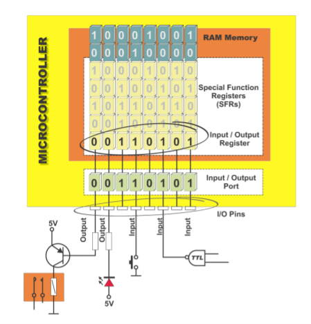
Unit-48051 Interfacing and Applications Q1) Explain the basics of I/O concepts?8051 microcontrollers have 4 I/O ports each of 8-bit, which can be configured as input or output. Hence, total 32 input/output pins allow the microcontroller to relate to the peripheral devices. Pin configuration, the pin can be configured as 1 for input and 0 for output as per the logic state. Port 0 − The P0 (zero) port is characterized by two functions − Input ConfigurationIf any pin of this port is configured as an input, then it acts as if it “floats”, i.e. the input has unlimited input resistance and in-determined potential.Output ConfigurationWhen the pin is configured as an output, then it acts as an “open drain”. By applying logic 0 to a port bit, the appropriate pin will be connected to ground (0V), and applying logic 1, the external output will keep on “floating”.To apply logic 1 (5V) on this output pin, it is necessary to build an external pullup resistor. Q2) Explain the I/O Port Operation?All 8051 microcontrollers have 4 I/O ports each comprising 8 bits which can be configured as inputs or outputs. Accordingly, in total of 32 input/output pins enabling the microcontroller to be connected to peripheral devices are available for use.Pin configuration, to know whether it is to be configured as an input (1) or an output (0), depends on its logic state. To configure a microcontroller pin as an input, it is necessary to apply a logic zero (0) to appropriate I/O port bit. In this case, voltage level on appropriate pin will be 0. To configure a microcontroller pin as an input, it is necessary to apply a logic one (1) to appropriate port. In this case, voltage level on appropriate pin will be 5V (as is the case with any TTL input).
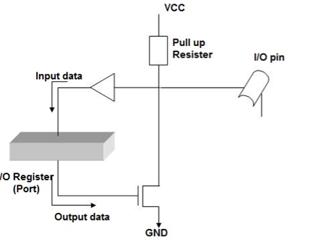
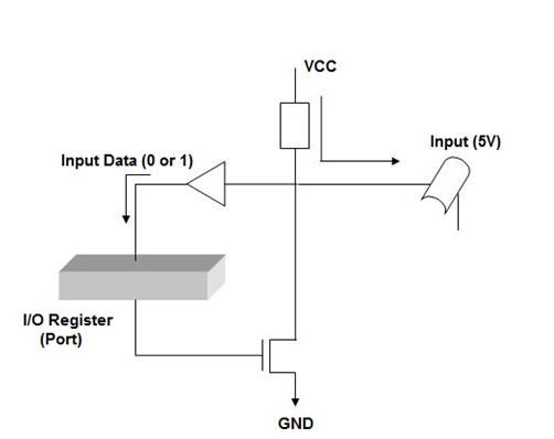
The figure above illustrates a simplified schematic of all circuits within the microcontroller connected to one of its pins. It refers to all the pins except those of the P0 port which do not have pull-up resistors built-in.
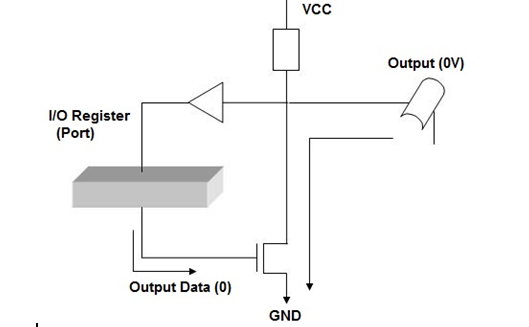
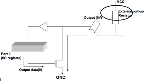
Output pin A logic zero (0) is applied to a bit of the P register. The output FE transistor is turned on, thus connecting the appropriate pin to ground.
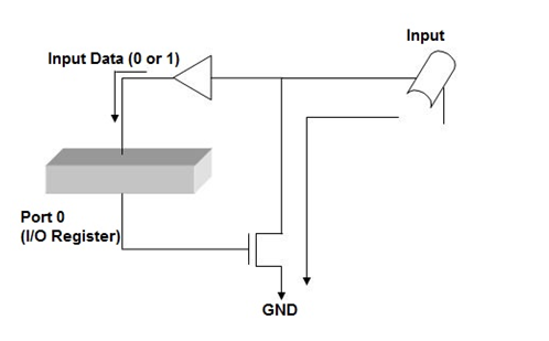
Input pin A logic one (1) is applied to a bit of the P register. The output FE transistor is turned off and the appropriate pin remains connected to the power supply voltage over a pull-up resistor of high resistance. Logic state (voltage) of any pin can be changed or read at any moment. A logic zero (0) and logic one (1) are not equal. A logic one (0) represents a short circuit to ground. Such a pin acts as an output. A logic one (1) is “loosely” connected to the power supply voltage over a resistor of high resistance. Since this voltage can be easily “reduced” by an external signal, such a pin acts as an input.
Port 0 The P0 port is characterized by two functions. If external memory is used then the lower address byte (addresses A0-A7) is applied on it. Otherwise, all bits of this port are configured as inputs/outputs.
If any pin of this port is configured as an input then it acts as if it “floats”. Such an input has unlimited input resistance and in determined potential.
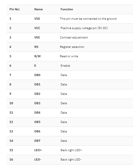
When the pin is configured as an output, it acts as an “open drain”. By applying logic 0 to a port bit, the appropriate pin will be connected to ground (0V). By applying logic 1, the external output will keep on “floating”. In order to apply logic 1 (5V) on this output pin, it is necessary to built in an external pull-up resistor. Port 1 P1 is a true I/O port, because it doesn't have any alternative functions as is the case with P0, but can be configured as general I/O only. It has a pull-up resistor built-in and is completely compatible with TTL circuits. Port 2 P2 acts similar to P0 when external memory is used. Pins of this port occupy addresses intended for external memory chip. This time it is about the higher address byte with addresses A8-A15. When no memory is added, this port can be used as a general input/output port showing features similar to P1.Port 3 All port pins can be used as general I/O, but they also have an alternative function. In order to use these alternative functions, a logic one (1) must be applied to appropriate bit of the P3 register. In terms of hardware, this port is similar to P0, with the difference that its pins have a pull-up resistor built-in. Q3) Explain the LCD interfacing of 8051?16×2 LCD module is a common type of LCD module that is used in 8051 based embedded projects. It consists of 16 rows and 2 columns of 5×7 or 5×8 LCD dot matrices. It is available in a 16 pin package with back light,contrast adjustment function and each dot matrix has 5×8 dot resolution. The pin numbers, their name and corresponding functions are shown in the table below.
VEE pin is meant for adjusting the contrast of the LCD display and the contrast can be adjusted by varying the voltage at this pin. This is done by connecting one end of a POT to the Vcc (5V), other end to the Ground and connecting the center terminal (wiper) of the POT to the VEE pin. If we make RS pin low and put a data on the data line, the module will recognize it as a command.R/W pin is meant for selecting between read and write modes. High level at this pin enables read mode and low level at this pin enables write mode.E pin is for enabling the module. A high to low transition at this pin will enable the module.DB0 to DB7 are the data pins. The data to be displayed and the command instructions are placed on these pins.The steps that has to be done for initializing the LCD display is given below and these steps are common for almost all applications.Send 38H to the 8 bit data line for initialization Send 0FH for making LCD ON, cursor ON and cursor blinking ON. Send 06H for incrementing cursor position. Send 01H for clearing the display and return the cursor. Sending data to LCD.The steps for sending data to the LCD module is given below.It is the logic state of these pins that make the module to determine whether a given data input is a command or data to be displayed.Make R/W low. Make RS=0 if data byte is a command and make RS=1 if the data byte is a data to be displayed. Place data byte on the data register. Pulse E from high to low. Repeat above steps for sending another data.
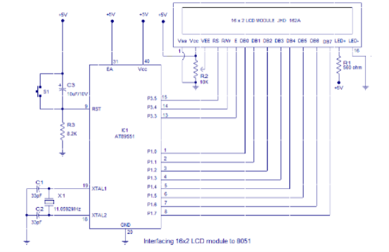
The circuit diagram given above shows how to interface a 16×2 LCD module with AT89S1 microcontroller. Capacitor C3, resistor R3 and push button switch S1 forms the reset circuitry. Ceramic capacitors C1,C2 and crystal X1 is related to the clock circuitry which produces the system clock frequency. P1.0 to P1.7 pins of the microcontroller is connected to the DB0 to DB7 pins of the module respectively and through this route the data goes to the LCD module. P3.3, P3.4 and P3.5 are connected to the E, R/W, RS pins of the microcontroller and through this route the control signals are transferred to the LCD module. Resistor R1 limits the current through the back light LED and so do the back light intensity. POT R2 is used for adjusting the contrast of the display. Program for interfacing LCD to 8051 microcontrollers is shown below.Program.MOV A,#38H // Use 2 lines and 5x7 matrixACALL CMNDMOV A,#0FH // LCD ON, cursor ON, cursor blinking ONACALL CMNDMOV A,#01H //Clear screenACALL CMNDMOV A,#06H //Increment cursorACALL CMNDMOV A,#82H //Cursor line one , position 2ACALL CMNDMOV A,#3CH //Activate second lineACALL CMNDMOV A,#49DACALL DISPMOV A,#54DACALL DISPMOV A,#88DACALL DISPMOV A,#50DACALL DISPMOV A,#32DACALL DISPMOV A,#76DACALL DISPMOV A,#67DACALL DISPMOV A,#68DACALL DISPMOV A,#0C1H //Jump to second line, position 1ACALL CMNDMOV A,#67DACALL DISPMOV A,#73DACALL DISPMOV A,#82DACALL DISPMOV A,#67DACALL DISPMOV A,#85DACALL DISPMOV A,#73DACALL DISPMOV A,#84DACALL DISPMOV A,#83DACALL DISPMOV A,#84DACALL DISPMOV A,#79DACALL DISPMOV A,#68DACALL DISPMOV A,#65DACALL DISPMOV A,#89DACALL DISPHERE: SJMP HERECMND: MOV P1,ACLR P3.5CLR P3.4SETB P3.3CLR P3.3ACALL DELYRETDISP:MOV P1,ASETB P3.5CLR P3.4SETB P3.3CLR P3.3ACALL DELYRETDELY: CLR P3.3CLR P3.5SETB P3.4MOV P1,#0FFhSETB P3.3MOV A,P1JB ACC.7,DELYCLR P3.3CLR P3.4RETEND Q4) Explain Keyboard Interfacing?Matrix keyboard is used for interfacing. It is designed with a rows and columns. These rows and columns are connected to the microcontroller through its ports of 8051. Generally we use 8*8 matrix key board. So only two ports of 8051 can be easily connected to the rows and columns of the keyboard. Whenever a key is pressed, a row and a column get shorted through that pressed key and all the other keys are left open. The bit in the port goes high which indicates the microcontroller that the key is pressed. By this high on the bit key in the corresponding column is identified.Once we are sure that one of key in the keyboard is pressed next our aim is to identify that key. To do this we firstly check particular row and then check the corresponding column on the keyboard.In order to check the row of the pressed key, one of the rows is made high by making one of bit in the output port of 8051 high. This is done until the row is found out. Once we get the row the next task is to detect the column of the pressed key. The column is detected by contents in the input ports with the help of a counter. The content of the input port is rotated with carry until the carry bit is set. The contents of the counter is compared and displayed in the display. This display is seven segment display and a BCD to seven segment decoder IC 7447.The BCD equivalent to the number of counter is sent through output part of 8051 displays the number of pressed key.
Figure 17. Keyboard interfacing with 8051 Steps:1.8051 has 4 I/O ports P0 to P3 each with 8 I/O pins, P0.0 to P0.7,P1.0 to P1.7, P2.0 to P2.7, P3.0 to P3.7. The one of the ports P1 means P1.0 to P1.7 serve as an i/p port for 8051. Port P0 serves as an o/p port of 8051 and port P2 is used for displaying the number of pressed key.2.Make all rows of port P0 high so that it gives high signal when key is pressed.3.See if any key is pressed by scanning port P1 and by checking all columns for non- zero condition.4.If any key is pressed, then identify which key is pressed make one row high at a time.5.Initiate a counter to hold the count so that each key is counted.6.Check port P1 for nonzero condition. If any nonzero number is there in [accumulator], start column scanning by following step 9.7.Otherwise make next row high in port P1.8.Add a count of 08h to the counter to move to the next row by repeating steps from step 6. 9.If any key pressed is found, the [accumulator] content is rotated right through the carry until carry bit sets, while doing this increment the count in the counter till carry is found.10. Move the content in the counter to display in data field or to memory location 11.To repeat the procedures, go to step 2. Program:Start of main program: to check that whether any key is pressedstart: mov a,#00h mov p1,a ;making all rows of port p1 zero mov a,#0fh mov p1,a ;making all rows of port p1 highpress: mov a,p2 jz press ;check until any key is pressed after making sure that any key is pressed. mov a,#01h ;make one row high at a time mov r4,a mov r3,#00h ;initiating counternext: mov a,r4 mov p1,a ;making one row high at a time mov a,p2 ;taking input from port A jnz colscan ;after getting the row jump to check column mov a,r4 rl a ;rotate left to check next mov r4,a mov a,r3 add a,#08h ;increment counter by 08 count mov r3,a sjmp next ;jump to check next row after identifying the row to check the column following steps are followedcolscan: mov r5,#00h in:rrc a ;rotate right with carry until get the carry jc out ;jump on getting carry inc r3 ;increment one count jmp in out: a,r3 da a ;decimal adjust the contents of counter before display mov p2,a jmp start ;repeat for check next key. Q5) Explain Parallel and Serial ADC?ADC devicesAnalog-to-digital converters are among the most widely used devices for data acquisition. We need an analog-to-digital converter to translate the analog signals to digital numbers so that the microcontroller can read and process them. An ADC has n-bit resolution where n can be 8, 10, 12, 16 or even 24 bits. The higher-resolution ADC provides a smaller step size, where step size is the smallest change that can be discerned by an ADC. Conversion time is defined as the time it takes the ADC to convert the analog input to a digital (binary) number.The ADC0804 1C is an 8-bit parallel ADC in the family of the ADC0800 seriesCSChip select is an active low input used to activate the ADC0804 chip. To access the ADC0804, this pin must be low.RD (read)This is an input signal and is active low. The ADC converts the analog input to its binary equivalent and holds it in an internal register. RD is used to get the converted data out of the ADC0804 chip. When CS = 0, if a high-to-low pulse is applied to the RD pin, the 8-bit digital output shows up at the DO – D7 data pins. The RD pin is also referred to as output enable (OE). WR (write; a better name might be “start conversion”)This is an active low input used to inform the ADC0804 to start the conversion process. If CS = 0 when WR makes a low-to-high transition.
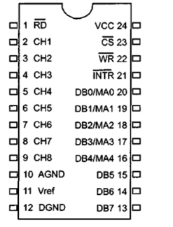
The ADC0848 has a resolution of 8 bits. It is an 8-channel ADC, thereby
CSChip select is an active low input used to activate the 848 chip. To access the 848, this pin must be low.RD (read)RD is an input signal and is active low. ADC converts the analog input to its binary equivalent and holds it in an internal register. RD is used to get the converted data out of the 848 chip. When CS = 0, if the RD pin is asserted low, the 8-bit digital output shows up at the DO – D7 data pins. The RD pin is also referred to as output enable (OE).VrefVref is an input voltage used for the reference voltage. The voltage connected to
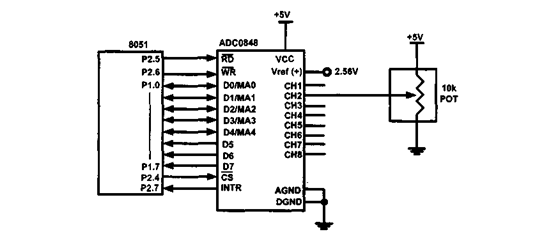
this pin dictates the step size. For the ADC0848, the step size is Vref/256since it is an 8-bit ADC and 2 to the power of 8 gives us 256 steps. For example, if the analog input range needs to be 0 to 4 volts, Vref is connected to 4 volts.That gives 4 V/256 = 15.62 mV forthe step size. DBO – DB7DBO – DB7 are the digital data output pins. With a DO – D7 output, the 848 must be an 8-bit ADC. The step size, which is the smallest change, is dictated by the number of digital outputs and the Vref voltage. To calculate the output voltage, we use the following formula:Dout = Vin/step size where Dout = digital data output (in decimal), Vin = analog input voltage and stepsize (resolution) is the smallest change, which is VTef/256 for an 8-bit ADC. The following is a summary of the connection between the 8051 and the ADC0848 as shown in Figure. P1.0 – P1.7 D0-D7 of ADC ; Channel Selection (out) and read(in)P2.7 to INTR P2.7 as input P2.6 to WR P2.6 as output P2.5 to RD P2.5 as output P2 is an output when we select a channel, and it is an input when we read the converted data.
Figure . 8051 Connection to ADC0848 for Channel 2 Displaying ADC0848 data In order to display the ADC result on a screen or LCD, it must be converted to ASCII. To convert it to ASCII, however, it must first be converted to decimalProgramming AOC0848 in Assembly The following program selects channel 2, reads the data, and calls conversion and display subroutines. CS BIT P2.4 RD BIT P2.5 WR BIT P2.6 ORG 00H SETB INTR ; make INTR an input SETB CS ; set Chip Select high SET RD ; set Read High SET WR ; set Write high BACK : MOV P1,#0AH ; Chan 2 address NOP ; wait CLR CS ; chip select CLR WR ; write = LOW NOP ; make pulse width wide enough SETB RD ; bring out digital data MOV A,P1 ; get the value SETB CS ; de-select for next round ACALL CONVERT ; convert to ASCII ACALL DATA_DISPLAY ; display the data SJMP BACK Q6) Explain DAC interfacing?DAC (0808)In these systems microcontroller generates output, which is in digital form, but the controlling system requires analog signal as they don't accept digital data. There is a need to use DAC which converts digital data into equivalent analog voltage.
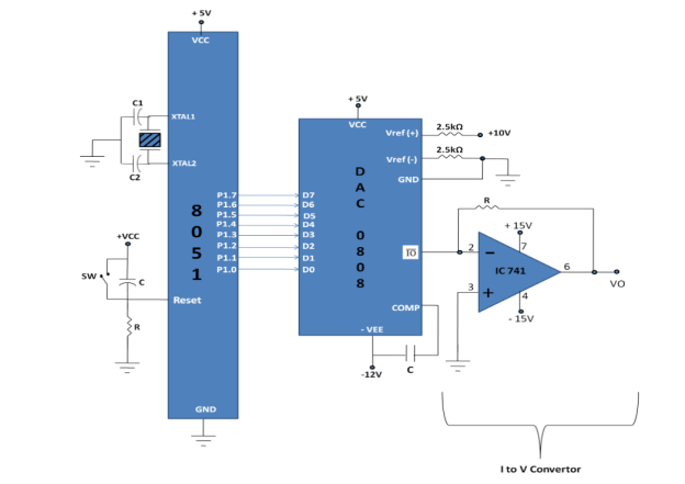
In the figure shown, we use 8-bit DAC 0808. This IC converts digital data into equivalent analog current. Hence, we require an I to V converter to convert this current into equivalent voltage. According to theory of DAC Equivalent analog output is given as:Vo = Vref[ D0/2 + D1/4 + D2/8 + D3/16 + D4/32 + D5/64+ D6/128+D7/256]
Ex:
1. IF data =00H [00000000] and Vref = 10VVo = 10[ 0/2 + 0/4+0/8+0/16+0/32+0/64+0/128+0/256] Therefore, V0= 0 Volts.
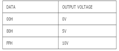
2. If data is 80H [10000000], and Vref = 10VVo = 10[1/2 + 0/4+0/8+0/16+0/32+0/64+0/128+0/256] Therefore, V0= 5 Volts.Different Analog output voltages for different Digital signal is given as:
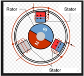
Figure . Interfacing 8051 with DAC 0808Program: ORG 000H MOV P1, #00H call squarwave call triwave call stairwave jmp repeatsquarwave: MOV P1,#FFH call delay2sec MOV P1,#00H call delay2sec rettriwave: MOV R7,#00Htriwave1: MOV P1,R7 inc R7 cjne R7, #FFH, triwave1 MOV R7, #FFhTriwave2: MOV P1, R7 djnz R7, triwave2 RETStairwave: MOV P1, #00H call delay2sec MOV P1, #20H Call delay2sec MOV P1, #40H Call delay2sec RETdelay1sec: MOV R0,#10del2 : MOV R1,#250del1: MOV R2,#250 DJNZ R2,$ DJNZ R1,del2 DJNZ R0,del1 RETDelay2sec: MOV R0,#20del2 : MOV R1,#250del1: MOV R2,#250 DJNZ R2,$ DJNZ R1,del21 DJNZ R0,del22 RET END Q7) Explain Stepper Motor? Stepper motors is mainly used to translate electrical pulses into mechanical movements. They are used in some disk drives, dot matrix printers. The main advantage of using the stepper motor is the position control. Stepper motors generally have a permanent magnet shaft (rotor), and it is surrounded by a stator.
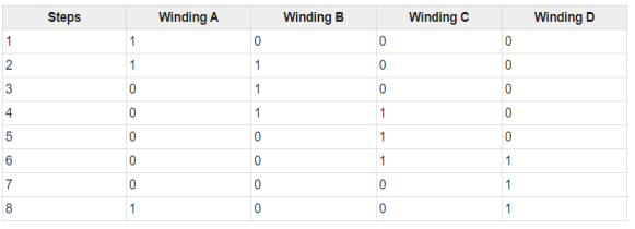
Figure. Stepper Motor Parameters of stepper motors:Step Angle - The step angle is the angle at which the rotor moves when one pulse is applied as an input of the stator. This parameter is used to determine the positioning of a stepper motor. Steps per Revolution - This is the number of step angles required for a complete revolution. The formula is 360° /Step Angle. Steps per Second - This parameter is used to measure number of steps covered in each second. RPM - The RPM is the Revolution Per Minute. It measures the frequency of rotation. We can measure the number of rotations in one minute. The relation between RPM steps per revolution and steps per second is Steps per second = rpm x steps per revolution / 60 Q8) Explain Stepper motor interfacing?Port P0 of 8051 is used for connecting the stepper motor. HereULN2003 is used. This is basically a high voltage, high current Darlington transistor array. Each ULN2003 has seven NPN Darlington pairs. It can provide high voltage output with common cathode clamp diodes for switching inductive loads.The Unipolar stepper motor works in three modes.Wave Drive Mode: In this mode, one coil is energized at a time. So all four coils are energized one after another. This mode produces less torque than full step drive mode.
Full Drive Mode: In this mode, two coils are energized at the same time. This mode produces more torque. Here the power consumption is also high.
Half Drive Mode: In this mode, one and two coils are energized alternately. At first, one coil is energized then two coils are energized. This is basically a combination of wave and full drive mode. It increases the angular rotation of the motor.
Figure 25. Interfacing Stepper Motor with 8051 Program:#include<reg51.h>sbit LED_pin = P2^0; //set the LED pin as P2.0void delay(int ms){ unsigned int i, j; for(i = 0; i<ms; i++){ // Outer for loop for given milliseconds value for(j = 0; j< 1275; j++){ //execute in each milliseconds ; } }}void main(){ int rot_angle[] = {0x0C,0x06,0x03,0x09}; int i; while(1){ //infinite loop for LED blinking for(i = 0; i<4; i++){ P0 = rot_angle[i]; delay(100); } }} Q9) Explain the applications of DC motor?Series Motors. The series DC motors are used where high starting torque is required and variations in speed are possible. ... Shunt Motors. ... Compound Motors. ... Separately Excited DC Generators. ... Shunt wound Generators. ... Series Wound Generators. Q10) Explain the interfacing of DC motor ?In order to generate delays 8051 has timers Timer-0 and Timer-1. They can be used for for delay purposes or for counting an event. To load 16-bit value in timers use two registers THx and TLx associated with timers. THx represents Timer High Byte and TLx represents Timer Low Byte. If I use Timer-0 then load value into TH0 and TL0 registers. Consider the following example:Calculate timer0 reload value needed to achieve timer delay of 20ms. The oscillator frequency is 11.0592 MHz.Delay value = Timer Delay / Timer Clock cycle duration = 20 x 10 -3 /6 ÷ 11.0592 x 10 6 = 36864Timer Reload Value = Maximum Register Count – Delay Value = 65535 – 36864= 28671 = 0 x 6FFFTherefore, timer O is loaded with TH0 = 0 x 6FH TH1 = 0 x FFHPWM is generated on Port-1 Pin#0. This is connected to L293D. To switch between different duty cycles use Push buttons. Each PUSH button corresponds to PWM of different duty cycle. Eight are connected to Port-2 and ninth is connected to Port-2. . At Pin 40 and 31 Apply 5V and Pin 18 and 19 connect crystal(11.0592). At pin20 ground it. Connect capacitors in parallel to crystal.
Figure 23. Dc Motor Speed Control using 8051 L293D motor driverDc motors need minimum 5 volts and 80 mA of current to work efficiently. 8051 microcontrollers cannot supply required amount of power as output on its gpio pins. Therefore, an external driver is required to accomplish this task. L293d motor driver is best to driver small dc motors In button statements Pwm_B_20=P2^1, 20 represents the duty cycle corresponding to button. Like in statement Pwm_B_60=P2^4, 60 represents the 60 us high time or 30% duty cycle. Delays greater than 200 us means 100% duty cycle. #include<reg51.h>sbit Pwm_Pin=P1^0;sbit Pwm_B_00=P2^0;sbit Pwm_B_20=P2^1;sbit Pwm_B_40=P2^2; sbit Pwm_B_50=P2^3;sbit Pwm_B_60=P2^4;sbit Pwm_B_80=P2^5;sbit Pwm_B_500=P2^6;sbit Pwm_B_800=P2^7;sbit Pwm_B_1000=P0^7;void Pwm_Low(){Pwm_Pin=0;TH0=0xFF;TL0=0x47;TR0=1; //Run Timer-0while(!TF0); //Wait for T0 Interrupt FlagTF0=0; //Clear Interrupt FlagTR0=0; //Stop Timer-0} void Pwm_High(){TR0=1; //Run Timer-0while(!TF0); //Wait for T0 Interrupt FlagTF0=0; //Clear Interrupt FlagTR0=0; //Stop Timer-0Pwm_Low();} void main(){ P0=0xFF; //**** Port-0 Declared Input P1=0x00; //**** Port-1 Declared Output P2=0xFF; //**** Port-2 Declared Input P3=0x00; //**** Port-3 Declared Output P0=0xFF; //**** Port-0 Declared Input TMOD=0x01; //Timer-0, As 16-bit Timer. while(1){ if(Pwm_B_00==0){ Pwm_Pin=1; TH0=0x00; TL0=0x00; Pwm_High();} else if(Pwm_B_20==0){ Pwm_Pin=1; TH0=0xFF; TL0=0xDA; Pwm_High();} else if(Pwm_B_40==0){ Pwm_Pin=1; TH0=0xFF; TL0=0xB5; Pwm_High();} else if(Pwm_B_50==0){ Pwm_Pin=1; TH0=0xFF; TL0=0x47; Pwm_High();} else if(Pwm_B_60==0){ Pwm_Pin=1; TH0=0xFE; TL0=0xD8; Pwm_High();} else if(Pwm_B_80==0){ Pwm_Pin=1; TH0=0xFE; TL0=0xB3; Pwm_High();} else if(Pwm_B_500==0){ Pwm_Pin=1; TH0=0xFC; TL0=0x65; Pwm_High();} else if(Pwm_B_800==0){ Pwm_Pin=1; TH0=0xFA; TL0=0x3C; Pwm_High();} else if(Pwm_B_1000==0){ Pwm_Pin=1; TH0=0xF8; TL0=0xCC; Pwm_High();} Else { } }
- Input/Output (I/O) pin − All the circuits within the microcontroller must be connected to one of its pins except P0 port because it does not have pull-up resistors built-in.
- Input pin − Logic 1 is applied to a bit of the P register. The output FE transistor is turned off and the other pin remains connected to the power supply voltage over a pull-up resistor of high resistance.
- When the external memory is used then the lower address byte (addresses A0A7) is applied on it, else all bits of this port are configured as input/output.
- When P0 port is configured as an output then other ports consisting of pins with built-in pull-up resistor connected by its end to 5V power supply, the pins of this port have this resistor left out.
|
|
|
|
|
|
|
|
|
The ADC0848 has a resolution of 8 bits. It is an 8-channel ADC, thereby
|
|
2. We can monitor the INTR pin of the ADC for end-of-conversion or we can wait a few milliseconds and then read the converted data.
|
In the figure shown, we use 8-bit DAC 0808. This IC converts digital data into equivalent analog current. Hence, we require an I to V converter to convert this current into equivalent voltage. According to theory of DAC Equivalent analog output is given as:Vo = Vref[ D0/2 + D1/4 + D2/8 + D3/16 + D4/32 + D5/64+ D6/128+D7/256]
Ex:
1. IF data =00H [00000000] and Vref = 10VVo = 10[ 0/2 + 0/4+0/8+0/16+0/32+0/64+0/128+0/256] Therefore, V0= 0 Volts.
2. If data is 80H [10000000], and Vref = 10VVo = 10[1/2 + 0/4+0/8+0/16+0/32+0/64+0/128+0/256] Therefore, V0= 5 Volts.Different Analog output voltages for different Digital signal is given as:
|
|
|
|
|
|
|
0 matching results found
