MICRO
Unit-8On-chip Peripherals Q1) Explain watch dog timer ?The internal watchdog of the MSP430 family is used either as a simple timer or as watchdog that ensures system integrity. The watchdog function is enabled after power-on reset or system reset. In case of any difficulties after start-up of MSP430, the watchdog will reset the system as often as it is needed for it to start successfully. A system running with MCLK = 3 MHz uses the watchdog for supervision of three functions.Power Fail — by the checking the 60 Hz AC line.Function 1 — A check is made if the software reaches this background part regularly Function 3 — A check is made if this interrupt handler is called regularly.Each supervised function sets a dedicated bit in RAM byte WDB in intervals less than 10.66 ms (power-up value of the watchdog with MCLK = 3 MHz) if everything is functioning normally. The main loop checks this byte (WDB) and resets the watchdog ONLY if all three bits are set (07h). If one of the functions fails, the watchdog is not reset and will therefore reset the system. Q2) Write a short note on comparator?
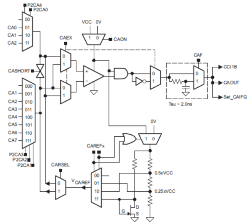
Figure . Comparator Operation:The comparator compares the analog voltages at the + and - input terminals. If + terminal is more positive than the – terminal the comparator output CAOUT is high. The comparator can be switched on or off using control bit CAON. The comparator should be switched off when not in use to reduce current consumption. When comparator is switched off CAOUT is always low. The analog input switches connect or disconnect the two comparator input terminals to associated port pins using P2CAx bits. Both comparator inputs can be controlled individually. The P2CAxbit allow:Application of external signal to the + and – terminals of the comparator. Routing of an internal reference voltage to an associated output port pin. The CAEX bit controls the input multiplexer, exchanging which input signals are connected to the comparators + and – terminals . The voltage reference generator is used to generate VCAREF which can be applied to either comparator input terminal. The CAREFx bits control the output of the voltage generator. The CARESEL bit selects the comparator terminal to which VCAREF is applied. Output Filter:The output of the comparator can be used with or without internal filtering. When the control bit CAF is set the output is filtered with an on-chip RC filter. Q3) Write a short note on Basic timer?
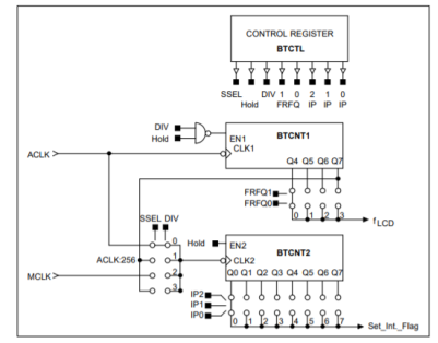
Figure . Basic Timer The basic timer supplies other peripheral modules with low frequency and control signals. The software can access both 8-bit counters.The control register BTCTL holds the flags to control or seelct the differential operational functions. The register BTCTL 8-bit counter BTCNT1 and the 8-bit counter BTCNT2 are under full control of the software. When the supply voltage is applied a reset of the device or watchdog timer overflow or any other operational condition occurs and all bts in the register hold an undefined or unchanged status. The user’s softeare usually configures the operational conditions of the Basic Timer1 during initialization. Q4) Explain Real Time Clock?
Figure . Real Time ClockReal Time clocks(RTC) are used in variety of applications from watches and clocks on time stamping events and generatig events. The geenral implementation of RTC is simple. It conists of timer/counter giving 1-second interrupts and small CPU routine to count the interrupts. The CPU can sleep or perform other functions between interrupts. The clock setup for RTC implementation uses LFXT1 oscillator in LF mode with 32768 Hz crystal. The otput of LFXT1 oscillator is selcted to source CLK . ACLK is then selected as the clock source for timer/counter that serves as the time base for RTC. The real time clock (RTC) module is used as general purpose 32 bit counter or as an RTC with calendar function selectable clock sources . It counts for seconds, minutes, hours and day of the week, day of the month and year in calendar mode. Q5) Write a short note on ADC?MSP stands for the mixed signal processor which means that many practical applications require analog inputs and analog output. There is a selection of analog to digital converter with a resolution of upto 10,12 bits and digital to analog converter. An analog to digital converter is an electronic circuit converts an analog input voltage into its digital representation. The output of the ADC is an integer that is proportional to the magnitude of the sampled analog voltage and relative to an internal or external reference voltage. Digital output = (Analog input voltage/ Reference voltage) x 2 ^(ADC bit size)
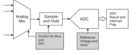
Figure . ADC 10The analog input circuitry in microcontroller starts with analog multiplexer to support multiple of analog input and any one of the input is allowed to further block to process the analog signal. The sample and hold circuitry holds the analog voltage and holds for ADC to complete conversion. The selction of the channel in the multiplexer and controlling sample and hold circuit are done by control registers. The output of sample and hold circuit is converted into corresponding digital output and its updated to ADC result memory as well as setting the flag. Q6) Write a short note on DAC?The basic method of DAC operation is to load DAC12_xDAT . Using the DAC12SELx bits of the control register , the actual trigger for the output is set. The device can be figured to output whenever the data register is written to, whenever the data register is written and the DAC enable is set or according to timers A and B. It is necessary to change the mode of SEL mode 0 in order to use interrupts with the DAC. The DAC can be interrupt enabled via the DAC control register and the interrupt eanble register. The fals is set whenever a conversion is complete. Also the DAC output can be grouped together to ensure that the output of both DACs appears simultaneously. When the unis are grouped both DAC_12xDAT registers must be written before the outputs appear. The device does not check whether you have changed the value updating with the same information. Q7) Explain LCD display application of MSP430?It is an electronic screen display module which finds wide range of applications. A 16x2 LCD display is very basic module commonly used in devices and circuits. These modules are preferred over seven segments because LCDs are economical easily programmable and have no limitation of displaying special and even custom characters animations and so on.
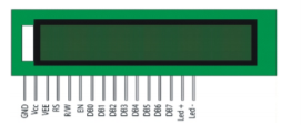
Figure. LCD DisplayA 16x2 LCD means it can display 16 characters per line and there are 2 such lines. In this LCD each character is displayed in 5x7 pixel matrix. This LCD has two registers, namely, Command and Data. The command register stores the command instructions given to the LCD. A command is an instruction given to LCD to do a predefined task like initializing it, clearing its screen, setting the cursor position, controlling display etc. The data register stores the data to be displayed on the LCD. The data is the ASCII value of the character to be displayed on the LCD.
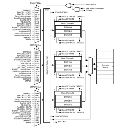
Figure. Interfacing #include<msp430g2211.h>#include”lcd16.h”#define EN BIT4 #define RS BIT5void Delay(volatile unsigned intx){volatile unsigned int i;for(x;x>1;x--){For(i=0;i<110;i++);}}void lcdcmd(unsigned char Data){P1OUT & = ~RS;// because sending command P1OUT & = ~EN;P1OUT & = ~RS;// because sending command P1OUT & = ~EN;P1OUT & = 0xF0; P1OUT | = ((Data>>4)&0x0F);P1OUT | =EN;Delay(2); P1OUT & = ~EN;P1OUT & = 0xF0; P1OUT | = ((Data>>4)&0x0F);P1 OUT |=EN;Delay(2);P1OUT&= ~EN;}void lcdData (unsigned char|){P1OUT | = RS;// because sending data P1OUT & = ~EN;P1OUT & = 0x0F;P1OUT |= (I>>4) &0x0F);P1OUT |=EN;Delay(2);P1OUT & = ~EN;P1OUT & = 0x0F;P1OUT |= (I &0x0F);P1OUT |=EN;Delay(2);P1 OUT & = ~EN;}void lcdinit(void){P1OUT = ~RS;// because sending data P1OUT & = ~EN;P1OUT & = 0x3;Delay(40)P1OUT |=EN;P1OUT & = ~EN;Delay(5)P1OUT | = EN;P1OUT  = ~EN;P1OUT |=EN;Delay(2);P1 OUT & = 0xF2;P1OUT |=EN;P1OUT & = ~EN;}lcdcmd90x28); // set data length 4 bit 2 lineDelay(250)lcdcmd(0x0E); //set display on cursor on blink on Delay(250)Lcdcmd(0x01) ; // clear lcdDelay(250)Lcdcmd(0x06)// cursor shift direction Delay(250)Lcdcmd(0x80);// set ram address Delay(250);}void main(void){WDTCTL = WDTPW+WDTHOLD;P1 DIR = 0xFF;P1 OUT = 0x00; lcdinit();prints(“EM MEDIA”);goto Xy(0,1) ;while(1);} Q8) Write a short note on DMA?The MSP430 is well suited to low-power applications, and DMA is useful facility to have to achieve this. The following devices in the MSP430 family support DMA: 5xxx, FG4xx(x), F261x, F16x(x) and F15x.The direct memory access (DMA) controller see block diagram allows movement of data from one memory address to another, across the entire address range, without CPU intervention.
Figure . DMA configuration DMA controller features:Three independent transfer channels ;Configurable DMA channel priorities DMA transfer cycle time:Requires only two MCLK clock cycles per transfer. Each byte/word transfer requires two MCLK cycles after synchronization and one cycle of wait tome after transfer. Byte or word and mixed byte/word transfer capability: Byte-to-byte; Word-to-word; Byte-to-word Word-to-byte (lower byte of the source word transfers). Block sizes up to 65535 bytes or words; Q9) Explain the clock system of MSP430?Clock sources availability depends on the version of MSP430 microcontroller.
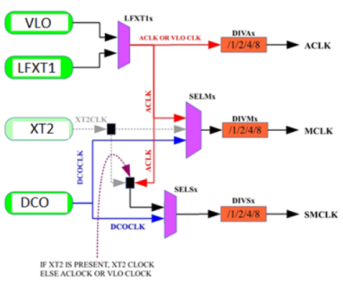
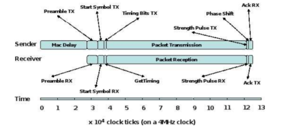
Figure 1. Clock System VLOCCLK- This is a very low power/low frequency internal oscillator that can produce a frequency of 10KHz.LFXT1CLK- (Low Frequency Crystal) – It is a crystal powered low/high frequency oscillator. It can work with either a 32Khz crystals that operate in the MHz range or external clock sources (400KHz to 16MHz range) XT2CLK(High frequency crystal)- This is a high frequency oscillator that can be used with standard crystals resonator or external clock sources in the 400Khz to 16 MHz range. DCOCLK- Integrated Digitally Controlled Oscillator do not use any external crystals. The DCO can generate a wide variety of frequencies ranging from few 100-kilo hertz to 10’s of MHz. It is default clock of the MSP430 after reset. The DCO clock frequency is temperature dependent. MSP430 produces 3 different clock signals using a combination of the oscillator sources. These clock signals can be used to various peripherals like CPU, Timers, ADC etc depending upon the requirements. MCLK- Known as main clock. It is fast high frequency clock usually used by CPU or other fast components like ADC10,ADC12, Watch Dog timer. MCLK can be sources either from LFT1CLK,DCO,VLO or XT2 oscillator. Clock signal can be divided by 1/2/4/8 using internal divider. SMCLK- Known as Sub Main Clock. It can be sources either from LFT1CLK,DCO,VLO or XT2 oscillator. Clock signal can be divided by 1/2/4/8 using internal divider. ACLK- known as Auxillary clock is slow,low frequency clock . It can only be sourced from LFT1CLK or VLO. Clock signal can be divided by 1/2/4/8 using internal divider. ALCK is active in all Low power modes except LPM4. Q10) Explain the Wireless sensor network with Chipcon RF interfaces of MSP430?The Tmote Sky uses a Texas Instruments MSP430 microprocessor running TinyOS, and a Chipcon SmartRF transceiver. TinyOS is an open-source platform specifically designed for the development of wireless sensor networks, and features a component-based architecture enabling rapid implementation despite the memory constraints of embedded systems. The Chipcon SmartRF transceiver utilizes the IEEE 802.15.4 specification, which includes both physical and MAC protocols, and allows packet routing independent of the microprocessor.The Tmote Sky utilizes an early IEEE 802.15.4 protocol for mesh networking using a Chipcon SmartRF CC2420 ZigBee-ready wireless transceiver. This transceiver is a low-cost solution for providing robust wireless communication in the unlicensed ISM band. The transceiver provides many desirable features, including a physical protocol, a MAC protocol, and AES encryption. These features are used by the Tmote Sky for its TinyOS mesh networking implementation . The Chipcon CC2420 transceiver interacts directly with TinyOS, allowing the Tmote platform to abstract the networking algorithms from the programmer. Simply specifying a destination node identifier in the NesC program allows TinyOS to transparently rout packets to the correct node, regardless of its location on the mesh network. Between the TinyOS code and the Chipcon transceiver, 11 the packets sent and received by the Tmote units appear similar to packets from any network. This includes the basic format of MAC, preamble, and data followed by an acknowledgement packet. This basic behaviour is outlined in a timing diagram depicted in Figure . This method of transmission is typical of most networks, wireless or otherwise, and speaks to the reliability of the Tmote Sky’s wireless networking capabilities.
Figure: Timing diagram of network transmission and reception
|
|
|
|
|
|
 = ~EN;P1OUT |=EN;Delay(2);P1 OUT & = 0xF2;P1OUT |=EN;P1OUT & = ~EN;}lcdcmd90x28); // set data length 4 bit 2 lineDelay(250)lcdcmd(0x0E); //set display on cursor on blink on Delay(250)Lcdcmd(0x01) ; // clear lcdDelay(250)Lcdcmd(0x06)// cursor shift direction Delay(250)Lcdcmd(0x80);// set ram address Delay(250);}void main(void){WDTCTL = WDTPW+WDTHOLD;P1 DIR = 0xFF;P1 OUT = 0x00; lcdinit();prints(“EM MEDIA”);goto Xy(0,1) ;while(1);} Q8) Write a short note on DMA?The MSP430 is well suited to low-power applications, and DMA is useful facility to have to achieve this. The following devices in the MSP430 family support DMA: 5xxx, FG4xx(x), F261x, F16x(x) and F15x.The direct memory access (DMA) controller see block diagram allows movement of data from one memory address to another, across the entire address range, without CPU intervention.
|
|
|
0 matching results found
