|

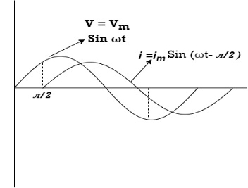
Consider a series R-L circuit connected across voltage source V= Vm sin wt Like some, I is the current flowing through the resistor and inductor due do this current-voltage drops across R and L R
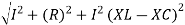
V = IR + I X L
|


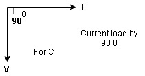
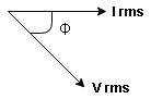
 Take current as the reference phasor: 1) for resistor current is in phase with voltage 2) for Inductor voltage leads current or current lags voltage by 90 0.
|
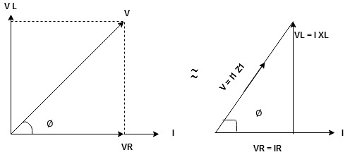
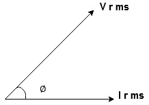
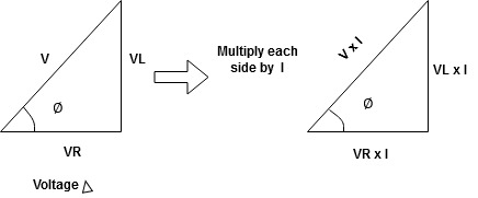
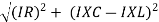
For voltage triangle Ø is the power factor angle between current and resultant voltage V and V =
V =
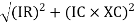
where Z = Impedance of circuit and its value is |


|

Rectangular form of Z = R+ixL and polar from of Z = (+ j X L + Where
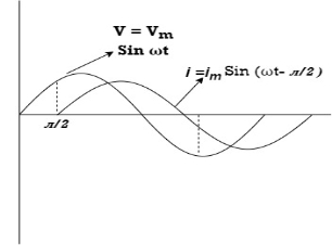
Current Equation : From the voltage triangle, we can sec. that voltage is leading current by Or i =
|


|
|
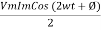
Power equation P = V .I. P = Vm Sin wt Im Sin wt – Ø P = Vm Im (Sin wt) Sin (wt – Ø) P = Since 2 sin A Sin B = Cos (A-B) – Cos (A+B) P =
①② | |
Average Power pang = Since ② term becomes zero because Integration of cosine come from 0 to 2ƛ
| |


|
From VI = VRI + VLI B Now cos Ø in
Similarly Sin
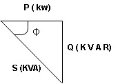
Apparent Power Average or true Reactive or useless power |


 for R L ekt.
|
|
V = Vm sin wt VR
|


|
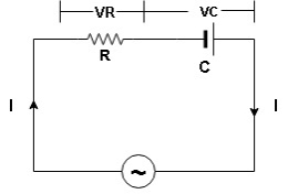
R and C R and C And C
|


|
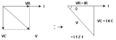
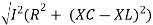
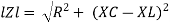
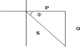
Where Ø is the power factor angle between current and voltage (resultant) V And from voltage V = V = V = V = Where Z = impedance of the circuit and its value is lZl = |


 by
by  as shown
|

The rectangular form of Z = R - jXc The polar form of Z = lZl L - Ø ( - Ø and –jXc because it is in the fourth quadrant ) where lZl = and Ø = tan -1 | ||
Current equation: from voltage triangle we can see that voltage is lagging current by Ø or current is leading voltage by Ø
Or i =
| ||


|
|
Power Equation: P = V. I P = Vm sin wt. Im Sin (wt + Ø) = Vm Im sin wt sin (wt + Ø) 2 Sin A Sin B = Cos (A-B) – Cos (A+B)
|

Average power
pang = since 2 terms integration of cosine wave from 0 to 2ƛ become zero
|


|
|

 L, VC = I
  C
C The voltage drops across XL> than XC
  VL> VC A
|

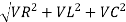
 Resultant voltage triangle
|
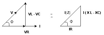
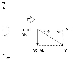
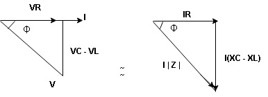
Now V = VR + VL + VC From voltage triangle V =
|


 : divide voltage
|
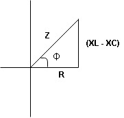
Rectangular form Z = R + j (XL – XC) Polor form Z = Where And Ø = tan-1 |


i = i = as VL
|
|


|
 XL :Since we have assured XC
  XL
XL  the voltage drops across XC
  than XL
 XC
XC  XL (A)
 voltage triangle considering condition (A)
|
 Resultant Voltage
|
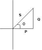
Now V = VR + VL + VC From voltage V = V =
|


 Impedance
  : Divide voltage
|

Polar form : Z = Where And Ø = tan-1 –
as VC since i =
|


 :
:
|
 they will cancel out each other and their resultant will have zero value.Hence resultant V = VR and it will be in phase with I as shown in the below phasor diagram.
|
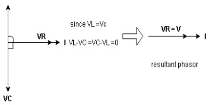
From the above resultant phasor diagram V =VR + IR Or V = I Because lZl + R Thus Impedance Z is purely resistive for XL = XC and circuit current will be in phase with source voltage. Since VR=V Øis zero when XL = XC i.e. pang = Vrms I rms cos Ø = 1 cos o = 1 maximum power will be transferred by the condition. XL = XC |


S= V × I Unit - Volte- Ampere (VA) In kilo – KVA
|
P = VI |

 ΦUnit –VA RIn kilo- KVAR
|

i.e. Φ.F= CosΦ |
|

Now Power factor = |


XL =
|


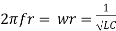
At a particle or frequency f=fr,the inductive and capacitive reactance are exactly Therefore, XL = XC ----at f=fr i.e. Therefore,
|
equal and
|


|

|
i.e. If. |


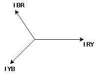
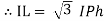
 take phase currents at reference as shown
|
|

Cos 300 =
|


|
|
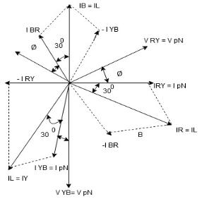
Inductive Reactance, XL. XL = 2 π f L = 2π x 50 x 0.15 = 47.13 Ω
Capacitive Reactance, XC. Xc = 1/ 2π fC = 1/ 2π x 50 x 100 x 10 -6 = 31.83 Ω
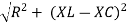
Circuit Impedance, Z. Z = [ R 2 + (XL – Xc) 2] ½ Z = [ 12 2 + (47.13 – 31.83) 2] ½ Z = [144 + 234] ½ = 19.4 Ω Circuits Current, I. I = Vs/ Z = 100/ 19.4 = 5.14 amps
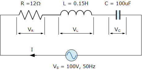
Voltages across the Series RLC Circuit, VR, VL, VC. VR = I x R = 5.14 x 12 = 61.7 volts VL = I x XL = 5.14 x 47.13 = 242.2 volts Vc = I x Xc = 5.14 x 31.8 = 163.5 volts |
Circuits Power factor and Phase Angle, θ. cos ɸ = R/Z = 12/ 19.4 = 0.619 cos -1 0.619 = 51.8 lagging Phasor Diagram. | ||
| ||
|
|
|
|


