UNIT 2
FET AND SCR
- Explain JFET Operations in detail.
- An FET is a three-terminal amplifying device.
- Its terminals are source, gate, and drain, which acts respectively like emitter, base, and collector of a normal transistor.
- There are two distinct families of FETs.
- The first is known as ‘junction-gate’ types of FETs or JUGFET or JFET.
- The second family is called ‘insulated-gate’ FETs or Metal Oxide Semiconductor FETs or MOSFET.
- ‘N-channel’ and ‘p-channel’ are the two versions of both types of FET.
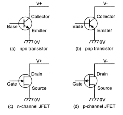
Operation
- N-channel FET consists of n-type semiconductor material with a drain terminal and a source terminal at opposite ends.
- A p-type gate is joined in the middle section of the n-type bar, thus forming a p-n junction.
- The drain terminal is connected to a positive supply and the gate is biased at a value that is negative (or equal) to the source voltage, thus reverse-biasing the JFET’s internal p-n junction, and accounting for its very high input impedance.
- When gate = 0V, a current flow from drain to source via a conductive ‘channel’ and the n-type bar is formed.
- When gate = negative , a high resistance region is formed within the junction, thus reduces the magnitude of the drain-to-source current and width of the n-type conduction channel.
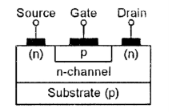
- Thus, the basic JFET passes maximum current when its gate bias is zero, and its current is reduced or ‘depleted’ when the gate bias is increased. It is thus known as a ‘depletion-type’ n-channel JFET.

2. Draw and explain I-V characteristics.
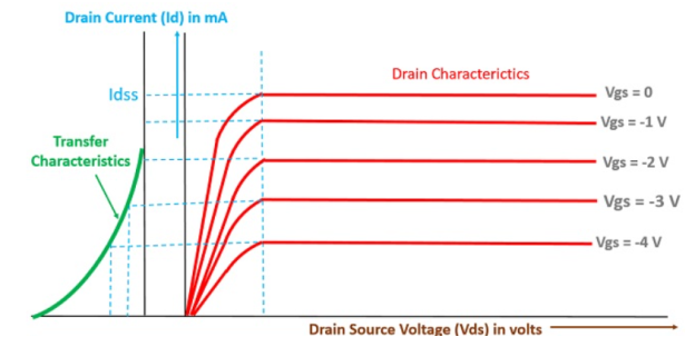
Output Characteristics or Drain Characteristics
- In the absence of external bias: In this case, as there is no voltage between gate and source terminal, thus, the drain current will flow from drain terminal to source terminal. We have already discussed in the working of JFET that majority charge carriers flow from source to drain and as a consequence of which the current flows from drain to source.
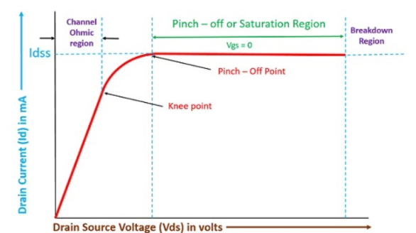
2. With external bias: When the external bias is applied to the gate-source terminal, the gate-source terminal becomes reversed bias externally. Obviously, if we are supplying an external voltage, then we can achieve the pinch-off point quite early as compared to the circuit which is not biased.
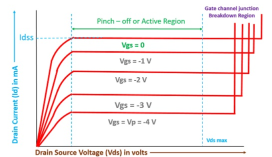
Transfer Characteristics
The transfer characteristics can be determined by observing different values of drain current with variation in gate-source voltage provided that the drain-source voltage should be constant. The transfer characteristics are just opposite to drain characteristics.
3. Explain MOSFET Operation in detail.
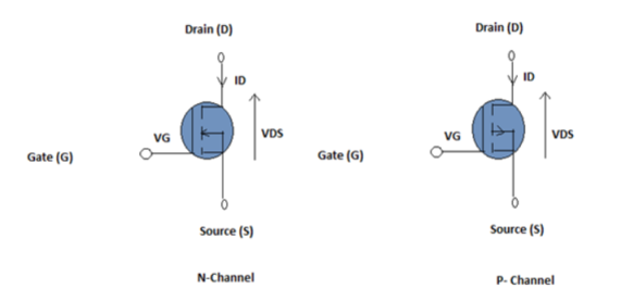
The MOSFET (Metal Oxide Semiconductor Field Effect Transistor) transistor is a semiconductor device which is widely used for switching and amplifying electronic signals in the electronic devices.
It is a core of integrated circuit and is designed and fabricated in a single chip because of its small size.
It is a four terminal device with source(S), gate (G), drain (D) and body (B) terminals.
The body of the MOSFET is connected to the source hence making it a three terminal device like field effect transistor. It can be used in both analog and digital circuits.
Operation
The MOSFET works by electronically varying the width of a channel along which charge carriers flow (electrons or holes).
The charge carriers enter the channel through source and exit via the drain.
The width of the channel is controlled by the gate voltage which is located between source and drain.
It is insulated from the channel near an extremely thin layer of metal oxide.
Function:
- Depletion Mode
When there is no voltage on the gate, the channel shows maximum conductance. When the voltage on the gate is either positive or negative, the channel conductivity decreases.
2. Enhancement Mode
The device does not conduct when there is no voltage on the gate. As the voltage increases on the gate, the better the device can conduct.
3. Draw MOSFET Characteristics.
MOSFET is seen to exhibit three operating regions viz.,
- Cut-Off Region
Cut-off region is a region in which the MOSFET will be OFF as there will be no current flow through it. In this region, MOSFET behaves like an open switch and is thus used when they are required to function as electronic switches. - Ohmic or Linear Region
Ohmic or linear region is a region where in the current IDS increases with an increase in the value of VDS. When MOSFETs are made to operate in this region, they can be used as amplifiers. - Saturation Region
In saturation region, the MOSFETs have their IDS constant inspite of an increase in VDS and occurs once VDS exceeds the value of pinch-off voltage VP. Under this condition, the device will act like a closed switch through which a saturated value of IDS flows. As a result, this operating region is chosen whenever MOSFETs are required to perform switching operations.

Fig: (a) Transfer Characteristics (b) Output Characteristics of NMOS
4.Explain NMOS and PMOS.
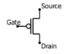
- The MOSFET (metal-oxide-semiconductor field-effect transistor) are of two types: PMOS (p-type MOS) and NMOS (n-type MOS).
- A new type of MOSFET logic is made combining both the PMOS and NMOS processes and is called as complementary MOS (CMOS).
- CMOS stands for “Complementary Metal Oxide Semiconductor”.
- It is one of the most popular technology in the chip design industry and is used today to form integrated circuits for various applications.
- Computer memories, CPUs and cell phones make use of this technology due to various advantages. This technology uses both P and N channel semiconductor devices.
NMOS
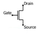
NMOS is built on a p-type substrate with n-type source and drain diffused on it. Here, the majority carriers are electrons. When a high voltage is applied to the gate, the NMOS conducts and when low voltage is applied to the gate, it does not conduct. NMOS is faster than PMOS, as the carriers are electrons that travel twice as fast as the holes.
PMOS
P-MOS consists of P-type Source and Drain diffused on an N-type substrate. Here, majority carriers are holes. When a high voltage is applied to the gate, the PMOS does not conduct and when a low voltage is applied, it conducts. These devices are more immune to noise than NMOS devices.

5. Explain CMOS inverter.

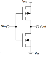
The inverter circuit as shown in the figure below. It consists of PMOS and NMOS FET. The input A serves as the gate voltage for both transistors.
The NMOS transistor has an input from Vss (ground) and PMOS transistor has an input from Vdd. The terminal Y is output. When a high voltage (~ Vdd) is given at input terminal (A) of the inverter, the PMOS becomes open circuit and NMOS switched OFF so the output will be pulled down to Vss.
When a low-level voltage (<Vdd, ~0v) applied to the inverter, the NMOS switched OFF and PMOS switched ON. So the output becomes Vdd or the circuit is pulled up to Vdd.
INPUT | LOGIC INPUT | OUTPUT | LOGIC OUTPUT |
0 V | 0 | Vdd | 1 |
Vdd | 1 | 0 v | 0 |
6. Draw VTC Characteristics for COMS.
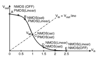
The VTC of complementary CMOS inverter is as shown in above Figure. The characteristics are divided into five regions of operations discussed as below :
Region A :
In this region the input voltage of inverter is in the range 0 Vin VTHn. Hence the NMOS is in cut-off and PMOS is in linear region and output voltage is VDD.
Region B :
In this region VTHn Vin < VDD2 in which p device is in linear region and n device is in saturation.
UNIT 2
UNIT 2
UNIT 2
FET AND SCR
- Explain JFET Operations in detail.
- An FET is a three-terminal amplifying device.
- Its terminals are source, gate, and drain, which acts respectively like emitter, base, and collector of a normal transistor.
- There are two distinct families of FETs.
- The first is known as ‘junction-gate’ types of FETs or JUGFET or JFET.
- The second family is called ‘insulated-gate’ FETs or Metal Oxide Semiconductor FETs or MOSFET.
- ‘N-channel’ and ‘p-channel’ are the two versions of both types of FET.

Operation
- N-channel FET consists of n-type semiconductor material with a drain terminal and a source terminal at opposite ends.
- A p-type gate is joined in the middle section of the n-type bar, thus forming a p-n junction.
- The drain terminal is connected to a positive supply and the gate is biased at a value that is negative (or equal) to the source voltage, thus reverse-biasing the JFET’s internal p-n junction, and accounting for its very high input impedance.
- When gate = 0V, a current flow from drain to source via a conductive ‘channel’ and the n-type bar is formed.
- When gate = negative , a high resistance region is formed within the junction, thus reduces the magnitude of the drain-to-source current and width of the n-type conduction channel.

- Thus, the basic JFET passes maximum current when its gate bias is zero, and its current is reduced or ‘depleted’ when the gate bias is increased. It is thus known as a ‘depletion-type’ n-channel JFET.

2. Draw and explain I-V characteristics.
Output Characteristics or Drain Characteristics
- In the absence of external bias: In this case, as there is no voltage between gate and source terminal, thus, the drain current will flow from drain terminal to source terminal. We have already discussed in the working of JFET that majority charge carriers flow from source to drain and as a consequence of which the current flows from drain to source.

2. With external bias: When the external bias is applied to the gate-source terminal, the gate-source terminal becomes reversed bias externally. Obviously, if we are supplying an external voltage, then we can achieve the pinch-off point quite early as compared to the circuit which is not biased.

Transfer Characteristics
The transfer characteristics can be determined by observing different values of drain current with variation in gate-source voltage provided that the drain-source voltage should be constant. The transfer characteristics are just opposite to drain characteristics.

3. Explain MOSFET Operation in detail.
The MOSFET (Metal Oxide Semiconductor Field Effect Transistor) transistor is a semiconductor device which is widely used for switching and amplifying electronic signals in the electronic devices.
It is a core of integrated circuit and is designed and fabricated in a single chip because of its small size.
It is a four terminal device with source(S), gate (G), drain (D) and body (B) terminals.
The body of the MOSFET is connected to the source hence making it a three terminal device like field effect transistor. It can be used in both analog and digital circuits.
Operation
The MOSFET works by electronically varying the width of a channel along which charge carriers flow (electrons or holes).
The charge carriers enter the channel through source and exit via the drain.
The width of the channel is controlled by the gate voltage which is located between source and drain.
It is insulated from the channel near an extremely thin layer of metal oxide.
Function:
- Depletion Mode
When there is no voltage on the gate, the channel shows maximum conductance. When the voltage on the gate is either positive or negative, the channel conductivity decreases.
2. Enhancement Mode
The device does not conduct when there is no voltage on the gate. As the voltage increases on the gate, the better the device can conduct.

3. Draw MOSFET Characteristics.
MOSFET is seen to exhibit three operating regions viz.,
- Cut-Off Region
Cut-off region is a region in which the MOSFET will be OFF as there will be no current flow through it. In this region, MOSFET behaves like an open switch and is thus used when they are required to function as electronic switches. - Ohmic or Linear Region
Ohmic or linear region is a region where in the current IDS increases with an increase in the value of VDS. When MOSFETs are made to operate in this region, they can be used as amplifiers. - Saturation Region
In saturation region, the MOSFETs have their IDS constant inspite of an increase in VDS and occurs once VDS exceeds the value of pinch-off voltage VP. Under this condition, the device will act like a closed switch through which a saturated value of IDS flows. As a result, this operating region is chosen whenever MOSFETs are required to perform switching operations.
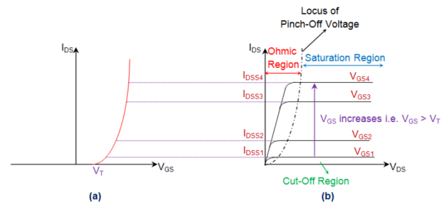
Fig: (a) Transfer Characteristics (b) Output Characteristics of NMOS
4.Explain NMOS and PMOS.
- The MOSFET (metal-oxide-semiconductor field-effect transistor) are of two types: PMOS (p-type MOS) and NMOS (n-type MOS).
- A new type of MOSFET logic is made combining both the PMOS and NMOS processes and is called as complementary MOS (CMOS).
- CMOS stands for “Complementary Metal Oxide Semiconductor”.
- It is one of the most popular technology in the chip design industry and is used today to form integrated circuits for various applications.
- Computer memories, CPUs and cell phones make use of this technology due to various advantages. This technology uses both P and N channel semiconductor devices.
NMOS
NMOS is built on a p-type substrate with n-type source and drain diffused on it. Here, the majority carriers are electrons. When a high voltage is applied to the gate, the NMOS conducts and when low voltage is applied to the gate, it does not conduct. NMOS is faster than PMOS, as the carriers are electrons that travel twice as fast as the holes.

PMOS
P-MOS consists of P-type Source and Drain diffused on an N-type substrate. Here, majority carriers are holes. When a high voltage is applied to the gate, the PMOS does not conduct and when a low voltage is applied, it conducts. These devices are more immune to noise than NMOS devices.
5. Explain CMOS inverter.
The inverter circuit as shown in the figure below. It consists of PMOS and NMOS FET. The input A serves as the gate voltage for both transistors.
The NMOS transistor has an input from Vss (ground) and PMOS transistor has an input from Vdd. The terminal Y is output. When a high voltage (~ Vdd) is given at input terminal (A) of the inverter, the PMOS becomes open circuit and NMOS switched OFF so the output will be pulled down to Vss.
When a low-level voltage (<Vdd, ~0v) applied to the inverter, the NMOS switched OFF and PMOS switched ON. So the output becomes Vdd or the circuit is pulled up to Vdd.
INPUT | LOGIC INPUT | OUTPUT | LOGIC OUTPUT |
0 V | 0 | Vdd | 1 |
Vdd | 1 | 0 v | 0 |
6. Draw VTC Characteristics for COMS.

The VTC of complementary CMOS inverter is as shown in above Figure. The characteristics are divided into five regions of operations discussed as below :
Region A :
In this region the input voltage of inverter is in the range 0 Vin VTHn. Hence the NMOS is in cut-off and PMOS is in linear region and output voltage is VDD.
Region B :
In this region VTHn Vin < VDD2 in which p device is in linear region and n device is in saturation.