UNIT 4
BJT
1. A 5.0V stabilized power supply is required to be produced from a 12V DC power supply input source. The maximum power rating PZ of the zener diode is 2W. Using the zener regulator circuit above calculate:
a). The maximum current flowing through the zener diode.
Maximum current = Watts/ Voltage =2W/5V =400mA
b). The minimum value of the series resistor, RS
 = 17.5 Ω
c). The load current IL if a load resistor of 1kΩ is connected across the zener diode.

d). The zener current IZ at full load.
Iz =Is -Il =440mA – 5mA = 395mA
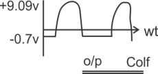
2. What would you expect to see displayed on oscilloscope connected across RL in the Limiter.

The diode is forward biased and conducts when then the i/pvtg goes below -0.7v so for the –ve limiter , the peak o/p vtg across RL can be determined by the following
Volt=(RL/R+RL) Vin
=(1k/100+1k)10v
= 1K/1.1K*10
=1*103/1.1*103*10
= 1*104/11*102*10
= 1*104*10-2*10
=10/11 10*10*10/11
Volt=10000/11=9.09V
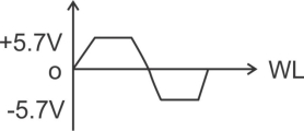
3. Fig shows a ckt combing a positive clipper with a-ve clipper. Determine the o/p vtg c/f

When the voltage at point A riches +5.7V diode A conducted and limits the waveform to +5.7v diode D2 does not conduct until the voltage reaches -5.7V
Therefore positive voltages above +5.7V & -ve voltages below -5.7V are clipped off
4. Explain operation of positive and negative clamper in detail.
1) Positive Clamper:-
Diagram:-

Assumptions:-
1) The V/p is a perfect sine waveform
2)The value of R& C are chosen such that the Line constant T=RC is large equal
3)The diode is an ideal one
4)TheRc time constant is much longer as compared to one cattle period ‘T’ of the input.
RC>100T
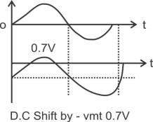
Operation :-I n the first negative half cycle after turning on the Ckt the diode acts as a closed S/W & charges the capacitor to peak ilpvtg VM with the polarity shown below

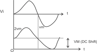
The diode reverse biased in both half cycle so it remains off.
2)Negative Clamper:-

In the first positive half cycle the capacitor will charge through the forward biased to peak vtgvm
The charging takes place very quickly as the diode resistances negligibly small
Once the capacitor charges to vm the diode is reverse biased and stops conducting.

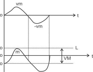
Diagram non ideal diode
5. An amplifier has a signal i/p Vtg. Vi of 0.25v and draws 1mA from the source. The amɤ delivers & v to a load at 10 mA. Determine the current Vtg and power gains. Also find the i/p resistance of this ampɤ what must be the open ckt. Vtg of the source Vs to provide an ampɤ i/p VtgVi of 0.25 v when the internal resistance of the source is 50 Ω?
Given Vi = 0.25v, Ii = 1 Ma, Vo = 8 v, Io = 10 mA, Rs = 50 Ω.
Solution:
Vtg gain Av = 
Current gain =
= 
Power gain AP = Av  = 32
= 32 
Input resistance Ri =  = 250
= 250
Open circuit Vtg of Vs
Vi = 
Vs = 
Vs = 
Vs = 0.3v
6. Explain MOSFET as a switch.
- MOSFET can act as a switch jest like a transistor a typical switching Ckt using N-channel EMOSFET shown below
- A positive going i/p pulse (high i/p) turns on the EMOSFET. Maxm drain current flows and the o/p Vtg drops from +VDD to RD ID (on). So the EMOSFET acts as closed switch.
- Similarly when the i/p is low (zero) no drain current and hence the o/p is equal to +VDD. So the EMOSFET acts as open s/w.
7. Explain N ans P type semi conductors.
N type Semiconductor:-
To increase the number of conduction band electrons intrinsic silicon , pentavalent imparity atoms are added. These are atoms with five valence electrons such as
i) arsenic (as)
Ii) phosphors (p)
Iii) Bismuth (Bi)
Iii) Antimony ( sb)
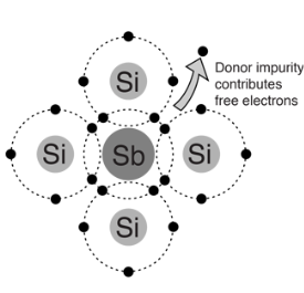
- Pentavalent impurity atom in a silicon crystal. An antimony (sb) impurity atom shown above-
- Each pentavalent atom forms covalent bonds with four adjustment silicon atoms, leaving one extra electron.
- The pentavalent atom gives up on electron, it often called a donor atom.
- Majority and minority carriers: - A type here means negative charge of an electron. Electron is called the majority carriers in n-type material.
- Hole in an n-type material are called minority carriers
P Type Semiconductor :-
To increase the number of holes in intrinsic silicon trivalent impurity atoms are added these are atoms with their valence electrons such as
i) Baron(B)
Ii) Indium(IN)
iii)Gallium(GO)
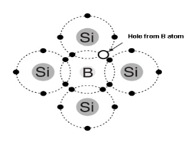
- Trivalent impurity atom in a silicon crystal structure. A) boron (B) impurity atom is shown in the center.
- The number of holes can be carefully controlled by the number of trivalent impurity atoms added to the silicon.
- A Hole created by the doping process is not accompanied by a conduction (free) electron.
- Trivalent Atom can take an electron it is often referred to as on accepted atom
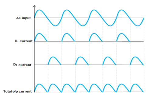
8. Draw and explain the operation of bridge rectifier.
It uses four individual rectifying diodes which are connected in a closed loop called “bridge” configuration to produce the desired output.
It does not require a special centre tapped transformer, hence reducing its size and cost. The single secondary winding is connected one side to the diode bridge network and the other side to the load.
The four diodes D1 to D4 are arranged in “series pairs” and only two diodes conduct current during each half cycle.
During the positive half cycle, diodes D1 and D2 conduct in series while diodes D3 and D4 are reverse biased producing current through the load.
During the negative half cycle, diodes D3 and D4 conduct in series and diodes D1 and D2 are switched “OFF” as they become reverse biased producing current through the load.
During each half cycle the current flows through two diodes instead of just one. The ripple frequency is now twice the supply frequency.

Output Waveform:
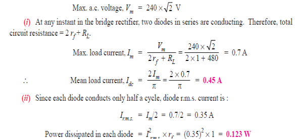
- 9. The four diodes used in a bridge rectifier circuit have forward resistances which may be considered constant at 1Ω and infinite reverse resistance. The alternating supply voltage is 240 V r.m.s. And load resistance is 480 Ω. Calculate (i) mean load current and (ii) power dissipated in each diode.
Solution :
