Aryabhatta Knowledge University (AKU)
Civil Engineering
Basic Electronics
Solved Exam Paper 2019
Question. Draw the diagram and explain the working of a full-wave rectifier with a filter.
The main function of full wave rectifier is to convert an AC into DC. As the name implies, this rectifier rectifies both the half cycles of the i/p AC signal, but the DC signal acquired at the o/p still have some waves. To decrease these waves at the o/p this filter is used.
In the full wave rectifier circuit using a capacitor filter, the capacitor C is located across the RL load resistor. The working of this rectifier is almost the same as a half wave rectifier. The only dissimilarity is half wave rectifier has just one-half cycles (positive or negative) whereas in full wave rectifier has two cycles (positive and negative).
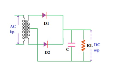 |
Once the i/p AC voltage is applied throughout the positive half cycle, then the D1 diode gets forward biased and permits flow of current while the D2 diode gets reverse biased & blocks the flow of current.
Throughout the above half cycle, the current in the D1 diode gets the filter and energizes the capacitor. But, the capacitor charging will occur just when the voltage which is applied is superior to the capacitor voltage. Firstly, the capacitor will not charge, as no voltage will stay among the capacitor plates. So when the voltage is switched on, then the capacitor will get charged immediately.
Throughout this transmission time, the capacitor gets charged to the highest value of the i/p voltage supply. The capacitor includes a highest charge at the quarter waveform in the positive half cycle. At this end, the voltage supply is equivalent to the voltage of the capacitor. Once the AC voltage begins falling & turns into less than the voltage of the capacitor, after that the capacitor begins discharging gradually.
As the i/p AC voltage supply gets the negative half-cycle, then the D1 diode gets reverse biased but the D2 diode is forward biased. Throughout the negative half cycle, the flow of current in the second diode gets the filter to charge the capacitor. But, the capacitor charging occurs simply while the applied AC voltage is superior to the voltage of the capacitor.
The capacitor in the circuit is not charged fully, so the charging of this does not occur instantly. Once the voltage supply becomes superior to the voltage of the capacitor, the capacitor gets charging. In both the half cycles, the flow of current will be in the similar direction across the RL load resistor. Thus we acquire either whole positive half cycle otherwise negative half cycle. In this case, we can get the total positive half cycle.
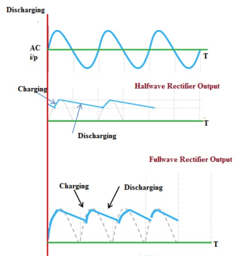 |
Thus, this is all about what is a filter and capacitor filter, halfwave rectifier with capacitor filter and full wave rectifier with capacitor filter and its input as well as output waveforms.
Question. Explain the working and application of photodiode
The photodiode construction can be done using two semiconductors like P-type & N-type. In this design, the formation of P-type material can be done from the diffusion of the P-type substrate which is lightly doped. So, the P+ ions layer can be formed because of the diffusion method. On the substrate of N-type, the N-type epitaxial layer can be grown.
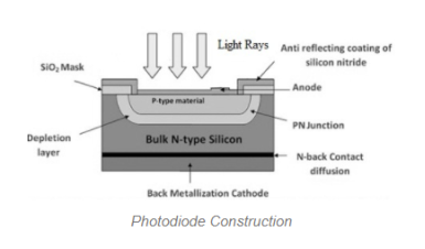 |
The development of a P+ diffusion layer can be done over the heavily doped N-type epitaxial layer. The contacts are designed with metals to make two terminals like anode and cathode. The front region of the diode can be separated into two types like active & non-active surfaces.
The designing of the non-active surface can be done with silicon dioxide (SiO2). On an active surface, the light rays can strike over it whereas, on a non-active surface, the light rays cannot strike. & the active surface can be covered through the material of anti-reflection so that the energy of light cannot lose and the highest of it can be changed into the current.
Working of Photodiode
The working principle of a photodiode is, when a photon of ample energy strikes the diode, it makes a couple of an electron-hole. This mechanism is also called the inner photoelectric effect. If the absorption arises in the depletion region junction, then the carriers are removed from the junction by the inbuilt electric field of the depletion region.
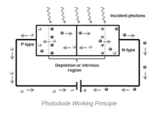 |
Therefore, holes in the region move toward the anode, and electrons move toward the cathode, and a photocurrent will be generated. The entire current through the diode is the sum of the absence of light and the photocurrent. So the absent current must be reduced to maximize the sensitivity of the device.
Applications of Photodiode
The applications of photodiodes involve similar applications of photodetectors like charge-coupled devices, photoconductors, and photomultiplier tubes.
These diodes are used in consumer electronics devices like smoke detectors, compact disc players, and televisions and remote controls in VCRs.
In other consumer devices like clock radios, camera light meters, and street lights, photoconductors are more frequently used rather than photodiodes.
Photodiodes are frequently used for exact measurement of the intensity of light in science & industry. Generally, they have an enhanced, more linear response than photoconductors.
Photodiodes are also widely used in numerous medical applications like instruments to analyze samples, detectors for computed tomography, and also used in blood gas monitors.
These diodes are much faster & more complex than normal PN junction diodes and hence are frequently used for lighting regulation and in optical communications
Question. Explain the construction, operation and characteristics of SCR
The silicon controlled rectifier (SCR) is a three terminal semiconductor switching device which can be used as a controlled switch to perform various functions such as rectification, inversion and regulation of power flow.
An SCR can handle currents upto several thousand amperes and voltages upto more than 1kV.
The SCR has appeared in the market under different names such as thyristor, thyrode transistor.
Like the diode, SCR is a unidirectional device,i.e. it will only conduct current in one direction only, but unlike a diode, the SCR can be made to operate as either an open-circuit switch or as a rectifying diode depending upon how its gate is triggered.
In other words, SCR can operate only in the switching mode and cannot be used for amplification.
Hence, it is extensively used in switching d.c. And a.c., rectifying a.c. To give controlled output, converting d.c. Into a.c. Etc.
 |
When a pn junction is added to a junction transistor, the resulting three pn junctions’ device is called a silicon controlled rectifier.
Fig.1(i) shows the construction of an SCR.
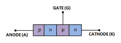 |
It is clear that it is essentially an ordinary rectifier (pn) and a junction transistor (npn) combined in one unit to form pnpn device.
Three terminals are taken; one from the outer p-type material called anode A, second from the outer layer of n-type material called cathode K and the third from the base of transistor section and is called gate G.
In the normal operating conditions of SCR, anode is held at high positive potential w.r.t. Cathode and gate at small positive potential w.r.t. Cathode.
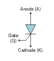 |
In a silicon controlled rectifier, load is connected in series with anode.
The anode is always kept at positive potential w.r.t. Cathode.
The working of SCR can be studied under the following two heads:
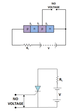
Fig.2 shows the SCR circuit with gate open i.e. no voltage applied to the gate.
 |
Under this condition, junction J2 is reverse biased while junction J1 and J3 are forward biased.
Hence, the situation in the junctions J1 and J3 is just as in a npn transistor with base open.
Consequently, no current flows through the load RL and the SCR is cut off.
However, if the applied voltage is gradually increased, a stage is reached when the reverse biased junction J2 breaks down.
The SCR now conducts heavily and is said to be in the ON state.
The applied voltage at which SCR conducts heavily without gate voltage is called Breakover voltage.
2. When gate is positive w.r.t. Cathode
The SCR can be made to conduct heavily at smaller applied voltage by applying a small positive potential to the gate as shown in fig.3.
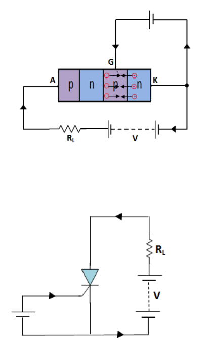 |
Now junction J3 is forward biased and junction J2 is reverse biased.
The electrons from n-type material start moving across junction J3 towards left whereas holes from p-type towards the right.
Consequently, the electrons from junction J3 are attracted across the junction J2 and gate current starts flowing .
As soon as the gate current flows, anode current increases.
The increased current in turn makes more electrons available at junction J2.
This process continues and in an extremely small time, junction J2 breaks down and the SCR starts conducting heavily.
Once SCR starts conducting, the gate loses all control. Even if gate voltage is removed, the anode current does not decrease at all.
The only way to stop conduction i.e. to bring the SCR in off condition, is to reduce the applied voltage to zero.
Question. Explain the working of common collector amplifier as a voltage buffer
Good transistor amplifiers essentially have the following parameters high gain, high input impedance, high bandwidth, high slew rate, high linearity, high efficiency, high stability, etc.
In the Common Collector transistor configuration, we use the collector terminal as common for both input and output signals. This configuration is also known as emitter follower configuration because the emitter voltage follows the base voltage. The emitter follower configuration is mostly used as a voltage buffer. These configurations are widely used in impedance matching applications because of their high input impedance.
Common collector amplifiers have the following circuit configurations.
● The input signal enters the transistor at the base terminal
● The input signal exits the transistor at the emitter terminal
● The collector is connected to a constant voltage, i.e. ground, sometimes with an intervening resistor
A simple common-collector amplifier circuit is shown in the figure below. The collector resistor Rc is unnecessary in many applications. In order to work transistor as an amplifier, it should be in the active region of its configuration.
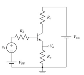 |
For that we set the quiescent point need to be set with the circuitry external to the transistor, the values of resistors Rc and Rb, and the DC voltage sources, Vcc and Vbb, have been chosen accordingly.
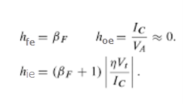
Once the circuit quiescent conditions have been calculated and it has been determined that the BJT is in the forward- active region of operation, the h-parameters are calculated below to form the small-signal model of the transistor.
 |
Question. Compute and explain common-emitter amplifier operating point and load line
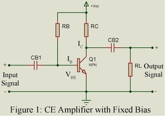
Figure 1 gives the basic circuit of CE amplifier using NPN transistor bias through use of resistor Rb. Here capacitor Cb1, acts as the coupling capacitor to couple the input signal to the base-to-emitter terminals of the transistor. One end of the input voltage Vi is at the ground potential. Vcc is the collector supply voltage which serves the additional function of providing the bias current IB. Under zero signal condition, Cb1 acts as an open circuit since the reactance of a capacitor is infinity at zero frequency (dc).
Thus, the capacitor Cbl acts as blocking capacitor. Normally Cb1 is chosen so large that at the lowest signal frequency, its reactance is small enough to be considered as a short circuit. Thus, capacitor Cb1 blocks dc voltage but passes a.c. Signal voltage. Similarly, capacitor Cb2 serves the same two functions. Thus, Cb2 works as coupling capacitor and feeds the amplified a.c. Signal to constitute the output voltage V0 across RL. Simultaneously Cb2 blocks the d.c. Voltage. Thus, the amplified output a.c. Voltage may be applied to the input of the next amplifier stage without affecting the bias of the next stage.
 |
For given collector characteristics and transistor biasing, selection of proper operating point involves selection of suitable values of Rc and Vcc.
Collector current Ic is a function of VCE and base bias current IB and may be put mathematically as,
 ….. (1)
Equation 1 represents the static output characteristic of the CE transistor for base current IB.
On applying Kirchhoff’s voltage law (KVL) to the collector circuit including only RC. (Excluding Cb2 and RL) We get,
 ….. (2)
Equation 2 represents a straight line having intercept Vcc on the voltage axis and intercept  on the current axis. The slope of this line equals
 . This line is referred to as the load line and represents the dynamic characteristic of the device. The zero-signal operating point must be suitably located on this load line. This, in turn, depends on the value If RL. If
 , RL can be neglected and then for large symmetrical input signal (base current in this case), the operating point P1 should be located in the centre of the dc load line. Vc and Ic are the zero-signal collector voltage and collector current respectively at the operating point. Next on application of a time varying signal, base current varies symmetrically on either side of IB1, the point of operating moves along dc load line symmetrically about the zero-signal operating point P1 and the instantaneous collector voltage and collector current vary approximately symmetrically about the zero-signal values Vc and Ic respectively.
Question. Compare between depletion type MOSFET and enhancement type MOSFET
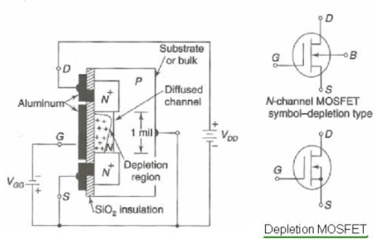 |
Figure-1 depicts construction of depletion type MOSFET. It also mentions circuit symbols of N-channel MOSFET of depletion type. Due to its construction if offers very high input resistance (about 1010 to 1015). Significant current flows for given VDS at VGS of 0 volt.
When a gate (i.e. one plate of capacitor) is made positive, the channel ((i.e. the other plate of capacitor) will have positive charge induced in it. This will result into depletion of majority carriers (i.e. electrons) and hence reduction in conductivity. Hence the curve similar to JFET is obtained as shown in figure-2.
As shown in the symbol here, the gate is insulated from the channel. For the P-channel type MOSFET symbol, the arrow will be reversed.
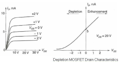 |
Figure-2 depicts drain characteristics and transfer curve of depletion type of MOSFET(N-channel).
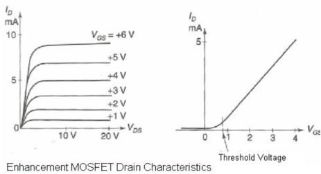 |
Figure-3 depicts construction of enhancement type MOSFET. It also mentions circuit symbols of N-channel MOSFET of enhancement type. Here the continuous channel does not exist from source to drain. Hence no current flows at zero gate voltage. Symbol depicts a broken channel between 'S' to 'D' terminals.
When positive voltage is applied to the gate, it will induce a channel by flowing minority carriers (i.e. electrons) from P-type bulk into the concentrated layer.
Figure-4 depicts drain characteristics and transfer curve of enhancement type of MOSFET (N-channel). As shown in the figure-4 minimum threshold voltage is needed for the flow of drain current to start.
This type of FET is ideal for switching applications. This is due to the fact that no gate voltage is needed to keep the device in 'off' state. Moreover the device can be powered ON with the application of the same polarity as drain terminal.
Following are the important comparison features between Depletion and Enhancement MOSFET types:
• Enhancement MOSFET does not conduct at 0 volt, as there is no channel in this type to conduct. Depletion MOSFET conducts at 0 volt. Moreover when positive cut-off gate voltage is applied to depletion MOSFET, hence it is less preferred.
• The depletion MOSFET does not have any kind of leakage currents such as gate oxide and sub threshold type.
• Depletion MOSFET logic operations are opposite to enhancement type of MOSFETs.
• Diffusion current (i.e. sub-threshold leakage current) exists in enhancement MOSFET while depletion MOSFET do not have any diffusion current.
Question. Explain the working of common base amplifier as a current buffer
An Amplifier circuit is used to increase the strength of the signal. The amplifier circuit uses the power supply to increase the signal strength. The amplification provided by the amplifier circuit is measured in terms of Gain of an amplifier. The gain of the amplifier is the ratio of output to input, which is always greater than one. Amplification does not alter frequency and waveform shape. In this article, we discuss the Common Base Amplifier circuit.
Gain of the Amplifier (A) = Output/(Input)
The ideal amplifier module has three important properties, namely, input impedance (Rin), output impedance (Rout) and of course amplification called as Gain(A). The amplifier module explains the general system of amplification with input and output signal. The impedance Rin increases the signal strength at gain A to produce the desired signal strength. Rin should be infinite and Rout should be zero.
The Common Emitter circuit is the most widely used configuration. This circuit has a grounded emitter. This circuit gives a medium level input impedance and output impedance. Voltage gain and current gain are medium, and the output reverses the input.
The Common collector circuit is widely used as a buffer. It is called the Emitter-follower. The emitter voltage follows that of the base. This gives a high input impedance and low output impedance. It has a grounded collector.
The Common base circuit provides low input impedance and high output impedance. The base of the transistor in this configuration is grounded. Input and output are in phase.
Common Base Amplifier Circuit
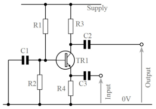
NPN and PNP transistors are used in Amplifier circuits. Both NPN and PNP have input provided at the emitter of the transistor and the output is taken at the collector of the transistor.
The below diagram shows how common base amplifier circuit is implemented.
The biasing constraints are same, but the applications of the signals are different. In this circuit, care has to be taken such that correct impedance match is provided to the input signal.
Characteristics of Common Base Amplifier Circuit
The following are the characteristics of the Common Base amplifier circuit.
● High voltage gain
● Low current gain
● Low power gain
● Input and output phase relation is 0o
● It has low input impedance
● It has high output impedance
 |
Question. Explain about the distortions present in the amplifier. List the advantages of negative feedback
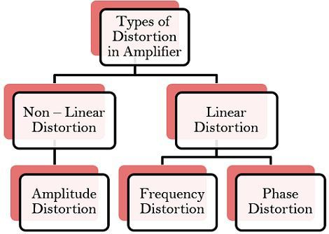
Distortion in Amplifier basically implies the variation in the waveform received at the output with respect to the applied input. The unwanted alterations generated during amplification is known as distortion.
A pure signal always has a single frequency component where voltage varies positive and negative by an equal amount. If this variation is less than full 360⁰ cycle, then it is said that the signal is distorted.
The amplified output must be an exact replica of the input. But practically such an ideal amplifier doesn’t exist. These undesired changes in the signal at the amplifier’s output are basiaclly termed as distortion in amplifier.
 |
For a distortion less output signal, dc biasing is required at the base or gate terminal. When dc biasing is employed, the signal is amplified over its entire cycle. The bias “Q point” must fall at the middle of the load line.
Thus, with such a “Q point” setting, type A amplification can be achieved. Reasons for signal distortion–
1. Due to incorrect biasing when the signal is not amplified for the entire cycle of the input signal then distortion occurs.
2. It also occurs in the case when the applied input signal is very large.
3. Distortion in amplifier sometimes results when the amplification is not linear over the complete frequency range.
As we are already aware of the fact that the amplifiers basically amplify small voltage signals in order to provide a larger signal at the output. After amplification, the output signal is the value obtained by the multiplication of amplifier’s gain with that of the input signal.
This is the reason why we get an amplified signal at the output of an amplifier. But the gain of amplifier i.e., β is different for the even similar type of transistor. Thus causing variation of “Q point” from a transistor to other.
 |
Advantages of negative feedback which are below:
The negative feedback has less frequency distortion.
It has highly stabilized gain.
It can control the step response of the amplifier.
It has less harmonic distortion.
It has less amplitude distortion.
It has less phase distortion.
The negative feedback reduces noise.
Input and output impedance can be modified as desired.
It can increase or decrease output impedance.
It has higher fidelity i.e. more linear operation.
Question. Explain the working of current series feedback amplifier with the help of block diagram
In the current series feedback circuit, a fraction of the output voltage is applied in series with the input voltage through the feedback circuit. This is also known as series-driven series-fed feedback i.e., a series-series circuit.
The following figure shows the block diagram of current series feedback, by which it is evident that the feedback circuit is placed in series with the output and also with the input.
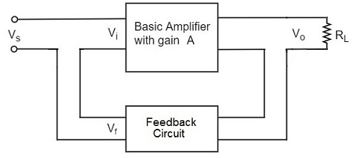 |
As the feedback circuit is connected in series with the output and the input as well, both the output impedance and the input impedance are increased.
Question. Describe the working of Wien bridge oscillator circuit
The Wien Bridge Oscillator is so called because the circuit is based on a frequency-selective form of the Wheatstone bridge circuit. The Wien Bridge oscillator is a two-stage RC coupled amplifier circuit that has good stability at its resonant frequency, low distortion and is very easy to tune making it a popular circuit as an audio frequency oscillator but the phase shift of the output signal is considerably different from the previous phase shift RC Oscillator.
The Wien Bridge Oscillator uses a feedback circuit consisting of a series RC circuit connected with a parallel RC of the same component values producing a phase delay or phase advance circuit depending upon the frequency. At the resonant frequency ƒr the phase shift is 0o. Consider the circuit below.
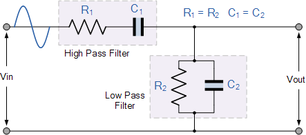 |
The above RC network consists of a series RC circuit connected to a parallel RC forming basically a High Pass Filter connected to a Low Pass Filter producing a very selective second-order frequency dependant Band Pass Filter with a high Q factor at the selected frequency, ƒr.
At low frequencies the reactance of the series capacitor (C1) is very high so acts a bit like an open circuit, blocking any input signal at Vin resulting in virtually no output signal, Vout. Likewise, at high frequencies, the reactance of the parallel capacitor, (C2) becomes very low, so this parallel connected capacitor acts a bit like a short circuit across the output, so again there is no output signal.
So there must be a frequency point between these two extremes of C1 being open-circuited and C2 being short-circuited where the output voltage, VOUT reaches its maximum value. The frequency value of the input waveform at which this happens is called the oscillators Resonant Frequency, (ƒr).
At this resonant frequency, the circuits’ reactance equals its resistance, that is: Xc = R, and the phase difference between the input and output equals zero degrees. The magnitude of the output voltage is therefore at its maximum and is equal to one third (1/3) of the input voltage as shown.
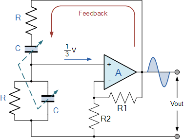 |
The output of the operational amplifier is fed back to both the inputs of the amplifier. One part of the feedback signal is connected to the inverting input terminal (negative or degenerative feedback) via the resistor divider network of R1 and R2 which allows the amplifiers voltage gain to be adjusted within narrow limits.
The other part, which forms the series and parallel combinations of R and C forms the feedback network and are fed back to the non-inverting input terminal (positive or regenerative feedback) via the RC Wien Bridge network and it is this positive feedback combination that gives rise to the oscillation.
The RC network is connected in the positive feedback path of the amplifier and has zero phase shift a just one frequency. Then at the selected resonant frequency, ( ƒr ) the voltages applied to the inverting and non-inverting inputs will be equal and “in-phase” so the positive feedback will cancel out the negative feedback signal causing the circuit to oscillate.
The voltage gain of the amplifier circuit MUST be equal too or greater than three “Gain = 3” for oscillations to start because as we have seen above, the input is 1/3 of the output. This value, ( Av ≥ 3 ) is set by the feedback resistor network, R1 and R2 and for a non-inverting amplifier this is given as the ratio 1+(R1/R2).
Also, due to the open-loop gain limitations of operational amplifiers, frequencies above 1MHz are unachievable without the use of special high frequency op-amps.
Question. Write the properties of ideal operational amplifier
Characteristics | Ideal Op Amp |
Infinite Voltage Gain | An ideal op amp will have infinite voltage gain. Op amps are devices that many times are used to function as amplifiers. A voltage is input into the op amp and as output, it produces the voltage amplified. An ideal op amp will produce mega-gain, practically, it will be able to produce infinite gain. It will amplify the signal infinite times over so that we can have as much gain as we'd ever need. |
Infinitely high input impedance | An ideal op amp will have infintely high input impedance. This will ensure that the op amp causes no loading in the circuit. The lower the input impedance, the more current that an op amp will draw. The higher the impedance, the lower the current that an op will draw. We want high input impedance so that the op amp doesn't disturb the original circuit by pulling current from it. To do this, we need infinitely high input impedance. |
Zero Output Impedance | An ideal op amp will have zero output impedance. When an op amp produces its output signal, we want the op amp to have zero voltage so that the maximum voltage will be transferred to the output load. Voltage is divided in a circuit according to the amount of impedance present in a circuit. Voltage drops across a component of higher impedance. In order for the voltage to drop across the output load, that load must be of greater impedance than the output of the op amp. This is why, ideally, we want the output impedance of the op amp to be zero |
Gain Independent of Frequency | In an ideal op amp, the gain that the op amp produces will be independent of frequency. This means that regardless of the frequency of the input signal going into the op amp, the gain that is produced will be constant and good across all frequencies. |
Zero Input Voltage Offset | In an ideal op amp, if no voltage is applied to the inverting and noninverting input pins, the op amp will output a voltage of 0, since there is no difference at all of the voltage applied to the 2 input pins. |
Positive and Negative Voltage Swings to Supply Rails | In an ideal op amp, the ac voltage which is fed into the op amp to be amplified will swing all the way up for the DC positive supply rail and all the way down for the DC negative supply rail, making 100% efficient use of the DC voltage supplied to an op amp. |
Output swings instantly to the correct value | In an ideal op amp, the output will swing instantly to the amplified voltage value. There will be no time delay between the time the voltage is input into the op amp till the time it is output. It will all be instantaneous. |