|
|
|
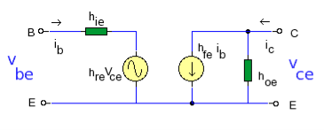
ic = hfe ib + hoe vceIf ib is held constant (ib=0) then hre and hoe can be solved:hre = vbe / vce | ib = 0
hoe = ic / vce | ib = 0Also if vce is held constant (vce=0) then hie and hfe can be solved:hie = vbe / ib | vce = 0
hfe = ic / ib | vce = 0These are the four basic parameters for a BJT in common emitter. Typical values are hre = 1 x10⁻⁴, hoe typical value 20uS, hie typically 1k to 20k and hfe can be 50 - 750. The H-parameters can often be found on the transistor datasheets. The table below lists the four h-parameters for the BJT in common base and common collector (emitter follower) mode.
|
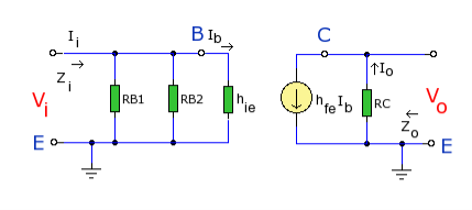
H-parameters are not constant and vary with temperature, collector current and collector emitter voltage. For this reason when designing a circuit the hybrid parameters should be measured under the same conditions as the actual circuit.The small signal parameter hreVce is often too small to be considered so the input resistance is just hie. Often the output resistance hoe is often large compared wi the the collector resistor RC and its effects can be ignored. The h-parameter equivalent model is now simplified and drawn below:
|
Input Impedance Zi
The input impedance is the parallel combination of bias resistors RB1 and RB2. As the power supply is considered short circuit at small signal levels then RB1 and RB2 are in parallel. RBB will represent the parallel combination:
As RBB is in parallel with hie then: Output Impedance Zo Voltage Gain Av as Ib = Vi / hie then:
Current Gain Ai
|
|
The current divider rule can be used for Ib:
At the output side, Io = hfe Ib re-arranging Io / Ib = hfe
If RBB >> hie then,
|
|
|
|
|
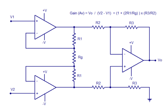
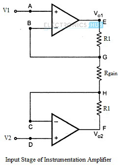
● The overall voltage gain of an instrumentation amplifier can be controlled by adjusting the value of resistor Rgain.
● The common mode signal attenuation for the instrumentation amplifier is provided by the difference amplifier.
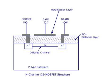
Question. With a neat diagram, explain the construction and operation of depletion MOSFET. Also write the drain and transfer characteristics.● Answer: The basic construction of n-channel depletion type MOSFET is provided in the figure shown above. A slab of p-type material is formed from a silicon base and is referred to as the substrate.
|
●
● It is the foundation upon which the device will be constructed.In some cases the substrate is internally connected to the source terminal. However, many discrete devices provide an additional terminal labelled SS, resulting in a four-terminal device, such as that appearing in the figure shown above.
● The source and drain terminals are connected through metallic contacts to n-doped regions linked by an n-channel as shown in the figure.The gate is also connected to a metal contact surface but remains insulated from the n-channel by a very thin silicon dioxide (SiO2) layer. SiO2 is a particular type of insulator referred to as a dielectric that sets up opposing electric fields within the dielectric when exposed to an externally applied field. The fact that the SiO2 layer is an insulating layer reveals the following fact:
|
●
● There is no direct electrical connection between the gate terminal and the channel of a MOSFET.
● It is the insulating layer of SiO2 in the MOSFET construction that accounts for the very desirable high input impedance of the device. In fact, the input resistance of a MOSFET is often that of the typical JFET, even though the input impedance of most JFETs is sufficiently high for most applications. The very high input impedance continues to fully support the fact that the gate current (IG) is essentially zero amperes for dc biased configuration
● The reason for the label metal-oxide-semiconductor FET is now fairly obvious: metal for the drain, source, and gate connections to the proper surface in particular, the gate terminal and the control to be offered by the surface area of the contact, the oxide for the silicon dioxide insulating layer, and the semiconductor for the basic structure on which the n-type and p-type regions are diffused. The insulating layer between the gate and channel has resulted in another name for the device: insulated gate FET or IGFET, although this label is used less and less in current literature.
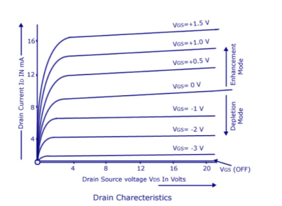
● In the figure, the gate-to-source voltage is set to zero volts by the direct connection from one terminal to the other and a voltage VDS is applied across the drain to source terminals. The result is an attraction for the positive potential at the drain by the free electrons of the n-channel and a current similar to that established through the channel of the JFET. In fact, the resulting current with VGS = 0 V continues to be labeled IDSS, as shown in the characteristics of depletion type MOSFET figure.
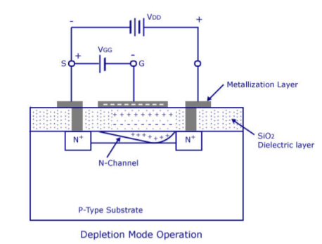
● In the figure, VGS has been set at a negative voltage such as 1 V. The negative potential at the gate will tend to pressure electrons toward the p-type substrate (like charges repel) and attract holes from the p-type substrate (opposite charges attract) as shown in the figure.
|
●
● Depending on the magnitude of the negative bias established by VGS, a level of recombination between electrons and holes will occur that will reduce the number of free electrons in the n-channel available for conduction. The more negative the bias, the higher the rate of recombination. The resulting level of drain current is therefore reduced with increasing negative bias for VGS as shown in the figure below for VGS = - 1 V, - 2 V, and so on, to the pinch-off level of 6 V.
● For positive values of VGS, the positive gate will draw additional electrons (free carriers) from the p-type substrate due to the reverse leakage current and establish new carriers through the collisions resulting between accelerating particles.As the gate to source voltage continues to increase in the positive direction, characteristics of depletion type MOSFET reveals that the drain current will increase at a rapid rate for the reasons listed above.
● The vertical spacing between the VGS = 0 V and VGS = 1 V curves of Fig. 5.25 is a clear indication of how much the current has increased for the 1-V change in VGS.Due to the rapid rise, the user must be aware of the maximum drain current rating since it could be exceeded with a positive gate voltage. That is, for the device of figure showing characteristics of depletion type MOSFET, the application of a voltage VGS = 4 V would result in a drain current of 22.2 mA, which could possibly exceed the maximum rating (current or power) for the device.
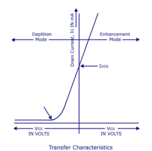
● As revealed above, the application of a positive gate-to-source voltage has “enhanced” the level of free carriers in the channel compared to that encountered with VGS = 0 V.For this reason the region of positive gate voltages on the drain or transfer characteristics is often referred to as the enhancement region, with the region between cutoff and the saturation level of IDSS referred to as the depletion region.
|
●
● It is particularly interesting and helpful that Shockley’s equation will continue to be applicable for the depletion type MOSFET characteristics in both the depletion and enhancement regions. For both regions, it is simply necessary that the proper sign be included with VGS in the equation and the sign be carefully monitored in the mathematical operations.
|
● Figure shows the schematic symbol for a DE-MOSFET. Just to the right of the gate is the thin vertical line representing the channel? The drain lead comes out from the top of the channel and the source lead connects to the bottom. The arrow is on the P-substrate and points to the N-material. In some applications, a voltage can be applied to the substrate for added control of drain current. For this reason, some DE-MOSFETs have four terminal leads. But in most applications, the substrate is connected to the source. Usually the substrate is connected to the source internally by the manufacturer. This results in a three terminal device whose schematic symbol is shown in figure.
● Schematic symbol for a three terminal P-channel DE-MOSFET device is shown in figure. The schematic symbol of a P-channel DE-MOSFET is similar to that of an N-channel DE-MOSFET, except that the arrow points outward.
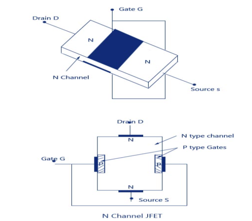
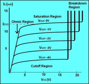
Question. With labelled diagram explain the construction of n-channel of JFET and also draw its characteristicsAnswer: The structure is quite simple. In an N-channel JFET an N-type silicon bar, referred to as the channel, has two smaller pieces of P-type silicon material diffused on the opposite sides of its middle part, forming P-N junctions, as illustrated in figure. The two P-N junctions forming diodes or gates are connected internally and a common terminal, called the gate terminal, is brought out. Ohmic contacts (direct electrical connections) are made at the two ends of the channel—one lead is called the Source terminal S and the other Drain terminal D.The silicon bar behaves like a resistor between its two terminals D and S. The gate terminal is analogous to the base of an ordinary transistor (BJT). It is used to control the flow of current from source to drain. Thus, source and drain terminals are analogous to emitter and collector terminals respectively of a BJT.In the figure above, the gate is P-region, while the source and the drain are N-regions. Because of this, a JFET is similar to two diodes. The gate and the source form one of the diodes, and the drain form the other diode. These two diodes are usually referred as the gate-source diode and the gate-drain diode. Since JFET is a silicon device, it takes only 0.7 volts for forward bias to get significant current in either diode.With the gate terminal not connected, and a potential applied (+ ve at the drain and – ve at the source), a current called the drain current, ID flows through the channel located between the two P-regions. This current consists of only majority carriers-electrons in this case. P-channel JFET is similar in construction to N-channel JFET except that P-type semiconductor material is sandwiched between two N-type junctions, as shown in figure. In this case majority carriers are holes.
|
|
|
|
|
● Can increase or decrease input impedance (depending on type of feedback).
● Can increase or decrease output impedance (depending on type of feedback).
● Reduces total distortion if sufficiently applied (increases linearity).
● Increases the bandwidth.
● Desensitizes gain to component variations.
● Can control step response of amplifier.
Cons:● May lead to instability if not designed carefully.
● Amplifier gain decreases.
● Input and output impedances of a negative-feedback amplifier (closed-loop amplifier) become sensitive to the gain of an amplifier without feedback (open-loop amplifier)—that exposes these impedances to variations in the open-loop gain, for example, due to parameter variations or nonlinearity of the open-loop gain.
● Changes the composition of the distortion (increasing audibility) if insufficiently applied.
The most widely preferred amplifier among the two types of the amplifier is the negative feedback amplifier. The characteristics of this amplifier are:● In the topology of the feedback amplifiers in the voltage series feedback the input impedance value increases and the output impedance decreases.● In the topology of the voltage shunt feedback, both the input and the output resistances values are decreases.● In the current series feedback circuits, both the input and the output resistances are increased because of its topology.● In the current shunt feedback topology, the amplifiers input resistance decreases and the output resistance decreases because of its connectivity of the input, output and feedback circuit.● In this way, the characteristics are defined based on the various topologies. Each topology defined has its significance of utilization.Simple amplifiers like the common emitter configuration have primarily low-order distortion, such as the 2nd and 3rd harmonics. In audio systems, these can be minimally audible because musical signals are typically already a harmonic series, and the low-order distortion products are hidden by the masking effect of the human hearing system.After applying moderate amounts of negative feedback (10–15 dB), the low-order harmonics are reduced, but higher-order harmonics are introduced. Since these are not masked as well, the distortion becomes audibly worse, even though the overall THD may go down. This has led to a persistent myth that negative feedback is detrimental in audio amplifiers, leading audiophile manufacturers to market their amplifiers as "zero feedback" (even when they use local feedback to linearize each stage).However, as the amount of negative feedback is increased further, all harmonics are reduced, returning the distortion to inaudibility, and then improving it beyond the original zero-feedback stage (provided the system is strictly stable).So the problem is not negative feedback, but insufficient amounts of it.Question. Explain positive clipping and negative clamping circuitsClampers can be broadly classified into two types. They are positive clampers and negative clampers.
|
|
