Back to Study material
BE

Aryabhatta Knowledge University (AKU)Electronics and Communications EngineeringBasic Electronics Solved Exam Paper 2019Question. Write the volt-ampere equation for a p-n junction diode and explain the meaning of each symbol. Describe the physical mechanism for Zener breakdownAnswer: A PN Junction Diode is one of the simplest semiconductor devices around, and which has the characteristic of passing current in only one direction only. However, unlike a resistor, a diode does not behave linearly with respect to the applied voltage as the diode has an exponential current-voltage ( I-V ) relationship and therefore cannot describe its operation by simply using an equation such as Ohm’s law.If a suitable positive voltage (forward bias) is applied between the two ends of the PN junction, it can supply free electrons and holes with the extra energy they require to cross the junction as the width of the depletion layer around the PN junction is decreased.By applying a negative voltage (reverse bias) results in the free charges being pulled away from the junction resulting in the depletion layer width being increased. This has the effect of increasing or decreasing the effective resistance of the junction itself allowing or blocking the flow of current through the diodes pn-junction.Then the depletion layer widens with an increase in the application of a reverse voltage and narrows with an increase in the application of a forward voltage. This is due to the differences in the electrical properties on the two sides of the PN junction resulting in physical changes taking place. One of the results produces rectification as seen in the PN junction diodes static I-V (current-voltage) characteristics. Rectification is shown by an asymmetrical current flow when the polarity of bias voltage is altered as shown below.Current I in a PN diode in related to the junction voltage VV by the relation given by equation,I = I_0 [e^{\dfrac{V}{\eta V_T}}-1]           ………..(1)Figure 1 gives the typical volt-ampere characteristic for a PN diode plotting above equation. With forward bias, the forward current remains essentially zero until the so called Cutin voltage VV of t diode is reached. This cutin voltage is defined as the voltage below which the forward current is less than 1% of the maximum rated current of the diode. This cutin voltage is also known as the turn-on voltage or threshold voltage. The cutin voltage varies with the semiconductor material and with the method of fabrication. Typically, the cutin voltage is about 0.2 volt for Ge diode and about 0.6 volt for Si diode. This higher value of cutin voltage in Si diode results mainly due to low value of IO.From figure 1 we observe that beyond the cutin voltage, the forward current increases rapidly with the increase of forward voltage. In the range of forward voltage, the applied voltage is much larger than VT (0.026 volt at 300 K) so that in above equation we may neglect 1 in comparison with e^{\dfrac{V}{\eta V_T}} and reduced to the following simpler formI = I_0 e^{\dfrac{V}{\eta V_T}}               ………(2)With small reverse bias, the reverse current increases with increases with increase in the magnitude of reverse bias. When the reverse bias magnitude exceeds several times VT, we may neglect e^{\dfrac{V}{\eta V_T}} is comparison with I and the reverse current becomes steady at value IO. with further increase of reverse voltage, the breakdown takes place and the reverse current then increases abruptly at an almost constant value of reverse voltage VZ.

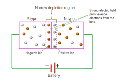
 The Zener breakdown occurs in heavily doped p-n junction diodes because of their narrow depletion region. When the reverse biased voltage applied to the diode is increased, the narrow depletion region generates a strong electric field.The Zener breakdown occurs in heavily doped p-n junction diodes because of their narrow depletion region.

 When a reverse biased voltage applied to the diode reaches close to Zener voltage, the electric field in the depletion region is strong enough to pull electrons from their valence band. The valence electrons which gains sufficient energy from the strong electric field of depletion region will breaks bonding with the parent atom. The valence electrons which break bonding with the parent atom will become free electrons. These free electrons carry electric current from one place to another place. At the Zener breakdown region, a small increase in voltage will rapidly increase the electric current.

       Zener breakdown occurs at low reverse voltage whereas avalanche breakdown occurs at high reverse voltage.

       Zener breakdown occurs in Zener diodes because they have very thin depletion region.

       Breakdown region is the normal operating region for a Zener diode.

       Zener breakdown occurs in Zener diodes with Zener voltage (Vz) less than 6V.

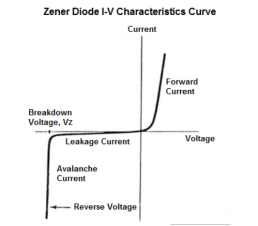
VI characteristics of Zener diodeThe VI characteristics of a Zener diode are shown in the below figure. When a forward biased voltage is applied to the Zener diode, it works like a normal diode. However, when a reverse biased voltage is applied to the Zener diode, it works in a different manner.The VI characteristics of a Zener diode are shown in the below figure.

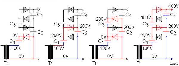
 The I-V Characteristics Curve of a Zener diode, shown below, is the curve which shows the current-voltage relationship of a Zener diode.Question. How does the reverse saturation current of a p-n diode vary with the temperature? How does the diode voltage (at constant current) vary with the temperature? Explain Answer: In a PN junction diode, the reverse current is due to the diffusive flow of minority electrons from the p-side to the n-side and the minority holes from the n-side to the p-side. Hence Is, reverse saturation current depends on the diffusion coefficient of electrons and holes. The minority carriers are thermally generated so the reverse saturation current is almost unaffected by the reverse bias but is highly sensitive to temperature changes. The reverse saturation current Is isWhere A is nearly constant independent of temperature and dependent on diffusion coefficients of electrons and holes. Eg is the band gap of the semiconductor, kB is the Boltzmann constant. ν is a constant; 1 for germanium and 2 for silicon; and T is the absolute temperature. Band gap of silicon is 1.12eV and that of germanium 0.66eVA-B curve: This curve shows the characteristics of diode for different temperatures in the forward bias. As we can see from the figure given above, that curve moves towards left as we increase the temperature. We know with increase in temperature, conductivity of semiconductors increase. When temperature is high, the electrons of the outermost shell take the thermal energy and become free. So conductivity increases with temperature. Hence with increase in temperature, the A-B curve would shift towards left i.e. curve would rise sharply and the breakdown voltage would also decrease with increase in temperature.A-C curve: This curve shows the characteristics of diode in the reverse biased region till the breakdown voltage for different temperatures. We know ni concentration would increase with increase in temperature and hence minority charges would increase with increase in temperature. The minority charge carriers are also known as thermally generated carriers and the reverse current depends on minority carriers only. Hence as the number of minority charge carriers increase, the reverse current would also increase with temperature as shown in the figure given on the previous page.      The reverse saturation current gets double with every 10 C increase in temperature.C-D curve: This curve shows the characteristics of a diode in reverse biased region from the breakdown voltage point onwards. As with increase in temperature, loosely bonded electrons are already free and to free the other electrons, it would take more voltage than earlier. Hence breakdown voltage increases with increase in temperature as depicted in the figure shown in the figure given on the previous page..B) Sketch the circuit of a voltage multiplier and explain its operation.A voltage multiplier is an electrical circuit that converts AC electrical power from a lower voltage to a higher DC voltage, typically using a network of capacitors and diodes.Voltage multipliers can be used to generate a few volts for electronic appliances, to millions of volts for purposes such as high-energy physics experiments and lightning safety testing. Assuming that the peak voltage of the AC source is +Us, and that the C values are sufficiently high to allow, when charged, that a current flows with no significant change in voltage, then the (simplified) working of the cascade is as follows:Illustration of the described operation, with +Us = 100 V
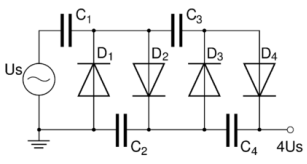
  • negative peak (Us): The C1 capacitor is charged through diode D1 to Us V (potential difference between left and right plate of the capacitor is Us)
  • positive peak (+Us): the potential of C1 adds with that of the source, thus charging C2 to 2Us through D2
  • Negative peak: potential of C1 has dropped to 0 V thus allowing C3 to be charged through D3 to 2Us.
  • Positive peak: potential of C2 rises to 2Us (analogously to step 2), also charging C4 to 2Us. The output voltage (the sum of voltages under C2 and C4) rises until 4Us is reached.
  • In reality more cycles are required for C4 to reach the full voltage. Each additional stage of two diodes and two capacitors increases the output voltage by twice the peak AC supply voltage.

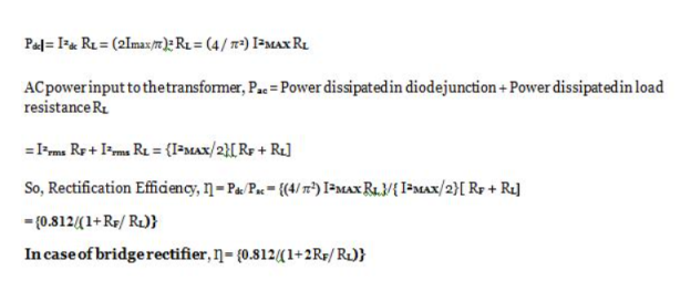
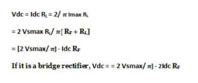
      Question .Define regulation. Derive the regulation equation for full-wave circuitAnswer: The circuit diagrams and waveforms we have given below will help you understand the operation of a bridge rectifier perfectly.  In the circuit diagram, 4 diodes are arranged in the form of a bridge. The transformer secondary is connected to two diametrically opposite points of the bridge at points A & C.  The load resistance RL is connected to bridge through points B and D.During the first half cycleDuring the first half cycle of the input voltage, the upper end of the transformer secondary winding is positive with respect to the lower end. Thus during the first half cycle diodes D1 and D3 are forward biased and current flows through arm AB, enters the load resistance RL, and returns back flowing through arm DC. During this half of each input cycle, the diodes D2 and D4 are reverse biased and current is not allowed to flow in arms AD and BC. The flow of current is indicated by solid arrows in the figure above. We have developed another diagram below to help you understand the current flow quickly. See the diagram below – the green arrows indicate the beginning of current flow from the source (transformer secondary) to the load resistance. The red arrows indicate the return path of current from load resistance to the source, thus completing the circuit.   During the second half cycleDuring the second half cycle of the input voltage, the lower end of the transformer secondary winding is positive with respect to the upper end. Thus diodes D2 and D4 become forward biased and current flows through arm CB, enters the load resistance RL, and returns back to the source flowing through arm DA. The flow of current has been shown by dotted arrows in the figure. Thus the direction of flow of current through the load resistance RL remains the same during both half cycles of the input supply voltage.  See the diagram below – the green arrows indicate the beginning of current flow from the source (transformer secondary) to the load resistance. The red arrows indicate the return path of current from load resistance to the source, thus completing the circuit.Peak Inverse Voltage of a Full wave bridge rectifier:Let’s analyses peak inverse voltage (PIV) of a full wave bridge rectifier using the circuit diagram. At any instant when the transformer secondary voltage attains positive peak value Vmax, diodes D1 and D3 will be forward biased (conducting) and the diodes D2 and D4 will be reverse biased (non conducting). If we consider ideal diodes in bridge, the forward biased diodes D1 and D3 will have zero resistance. This means voltage drop across the conducting diodes will be zero. This will result in the entire transformer secondary voltage being developed across load resistance RL.Thus PIV of a bridge rectifier = Vmax (max of secondary voltage)The different parameters are explained with equations below:Peak CurrentThe instantaneous value of the voltage applied to the rectifier is given asvs =  Vsmax Sin wt If the diode is assumed to have a forward resistance of RF ohms and a reverse resistance equal to infinity, the current flowing through the load resistance is given asi1 = Imax Sin wt and i2 = 0 for the first half cycleand i1 = 0 and i2 = Imax Sin wt for second half cycleThe total current flowing through the load resistance RL, being the sum of currents i1 and i2 is given asi = i1 + i2 = Imax Sin wt for the whole cycle.Where the peak value of the current flowing through the load resistance RL is given asImax = Vsmax/(2RF + RL)2.    Output CurrentSince the current is the same through the load resistance RL in the two halves of the ac cycle, magnitude of dc current Idc, which is equal to the average value of ac current, can be obtained by integrating the current i1 between 0 and pi or current i2 between pi and 2pi.

    3.    DC Output Voltage

    Average or dc value of voltage across the load is given as

    4.    Root Mean Square (RMS) Value of Output Voltage

    5.    Rectification Efficiency

    Power delivered to load,

    7.    Ripple Factor

    Form factor of the rectified output voltage of a full wave rectifier is given as

    So, ripple factor, γ =  (1.11 * 1.11  – 1) = 0.482

    8.    Regulation

    The dc output voltage is given as


    Question. Define ripple factor. Calculate the value of ripple factor for a half-wave rectifier circuit.Answer: The definition of the ripple factor is the ratio of the AC component’s RMS value and the DC component’s RMS value within the output of the rectifier. The symbol is denoted with “γ” and the formula of R.F is mentioned below.

     (R.F) = AC component’s RMS value / DC component’s RMS valueThus the R.F = I (AC) / I (DC)This is extremely significant while deciding the efficiency of rectifier output. The efficiency of the rectifier can be explained by the lesser R.F.Basically, the calculation of the ripple indicates the clarity of the resolved output. Therefore each effort can be made for diminishing the R.F.According to the definition of R.F, the whole load current RMS value can be given byIRMS = √I2dc + I2ac(or)Iac = √I2rms + I2dcWhen the above equation is divided by using Idc then we can get the following equation.Iac / Idc = 1/ Idc √I2rms + I2dcHowever, here Iac / Idc is the ripple factor formulaR.F = 1/ Idc √I2rms + I2dc = √ (Irms / Idc)2 -1Ripple Factor of Half Wave RectifierFor half-wave rectifier,Irms = Im/2Idc = Im/ πWe know the formula of R.F = √ (Irms / Idc)2 -1Substitute the above Irms & Idc in the above equation so we can get the following.R.F = √ (Im/2 / Im/ π)2 -1 = 1.21Here, from the above derivation, we can get the ripple factor of a half-wave rectifier is 1.21. Therefore it is very clear that AC. component surpasses the DC component within the half-wave rectifier output. It results in extra pulsation within the output. Consequently, this type of rectifier is ineffectively intended for changing AC to DC.

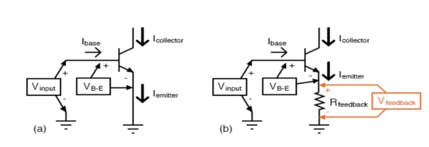
      Question. Explain the emitter feedback bias of a BJT transistor with the help of circuit diagramAnswer: Emitter feedback: A different method of introducing negative feedback into a circuit.This new feedback resistor drops voltage proportional to the emitter current through the transistor, and it does so in such a way as to oppose the input signal influence on the base-emitter junction of the transistor. Let’s take a closer look at the emitter-base junction and see what difference this new resistor makes in the figure below.With no feedback resistor connecting the emitter to ground in the figure below (a), whatever level of input signal (Vinput) makes it through the coupling capacitor and R1/R2/R3 resistor network will be impressed directly across the base-emitter junction as the transistor’s input voltage (VB-E). In other words, with no feedback resistor, VB-E equals Vinput. Therefore, if Vinput increases by 100 mV, then VB-E increases by 100 mV: a change in one is the same as a change in the other since the two voltages are equal to each other.Now let’s consider the effects of inserting a resistor (Rfeedback) between the transistor’s emitter lead and ground in Figure below (b).

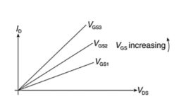
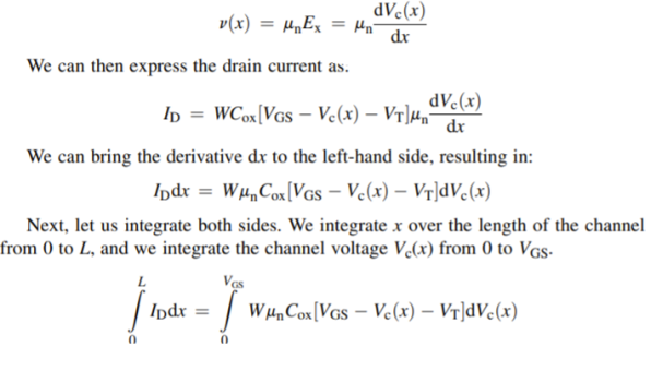
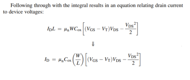
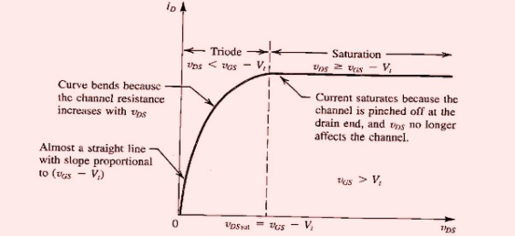
     (a) No feedback vs (b) emitter feedback. A waveform at the collector is inverted with respect to the base. At (b) the emitter waveform is in-phase (emitter follower) with base, out of phase with collector. Therefore, the emitter signal subtracts from the collector output signal.Note how the voltage dropped across Rfeedback adds with VB-E to equal Vinput. With Rfeedback in the Vinput—VB-E loop, VB-E will no longer be equal to Vinput. We know that Rfeedback will drop a voltage proportional to emitter current, which is in turn controlled by the base current, which is in turn controlled by the voltage dropped across the base-emitter junction of the transistor (VB-E). Thus, if Vinput were to increase in a positive direction, it would increase VB-E, causing more base current, causing more collector (load) current, causing more emitter current, and causing more feedback voltage to be dropped across Rfeedback. This increase of voltage drop across the feedback resistor, though, subtracts from Vinput to reduce the VB-E, so that the actual voltage increase for VB-E will be less than the voltage increase of Vinput. No longer will a 100 mV increase in Vinput result in a full 100 mV increase for VB-E, because the two voltages are not equal to each other.Consequently, the input voltage has less control over the transistor than before, and the voltage gain for the amplifier is reduced: just what we expected from negative feedback.In practical common-emitter circuits, negative feedback isn’t just a luxury; its a necessity for stable operation. In a perfect world, we could build and operate a common-emitter transistor amplifier with no negative feedback, and have the full amplitude of Vinput impressed across the transistor’s base-emitter junction. This would give us a large voltage gain. Unfortunately, though, the relationship between base-emitter voltage and base-emitter current changes with temperature, as predicted by the “diode equation.” As the transistor heats up, there will be less of a forward voltage drop across the base-emitter junction for any given current. This causes a problem for us, as the R1/R2 voltage divider network is designed to provide the correct quiescent current through the base of the transistor so that it will operate in whatever class of operation we desire (in this example, I’ve shown the amplifier working in class-A mode). If the transistor’s voltage/current relationship changes with temperature, the amount of DC bias voltage necessary for the desired class of operation will change. Question. In case of FET, how does the drain current vary with gate voltage in saturation region? Explain in detail.Answer: If there is current flowing in the MOSFET channel, we would expect a varying voltage along the length of the channel. Let us call this channel voltage Vc(x). Remember that no current will flow for gate to source (VGS) voltages less than the threshold voltage VT.  the charge per unit area under the gate in the channel as: a mobile gate charge exists only if the gate-source voltage exceeds the threshold voltage. The gate charge Qc(x) is the charge density (Coulombs/m2 ) at position x along the gate. The drain current is equal to:Where W is the width of the MOS device into the paper and v(x) is the “drift velocity” of the charges across the channel. If we assume a low electric field (and hence a long length device), the drift velocity is linearly related to the electric field with particle mobility as a proportionality constant, as:


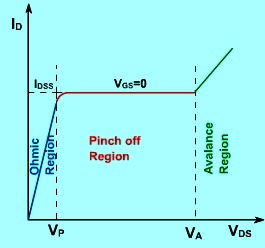
     Question. Explain the pinch off voltage Vp. Sketch the depletion region before and after the pinched-off in FET.Pinch off voltage: Pinch off voltage is the drain to source voltage after which the drain to source current becomes almost constant and JFET enters into saturation region and is defined only when gate to source voltage is zero.With the common-source common-source hook of a JFET to N channel, since gate voltage Vgs becomes more and more negative, the channel becomes narrower as the Mobile Depletion Zones invade the channel from the side.

     Finally, these Depletion Areas meet but the channel does not close! Instead, the channel becomes a long passage of constant width. Within this channel, avalanche breakdowns occur while small portions of the channel try to close. But every time this happens, a larger voltage appears through the closed portion, which brings the DZ back and opens the channel again.During pinch-off the channel behaves very strangely: it is no longer a resistance. Instead, when the drain-source Vds voltage increases, the conductive channel grows physically for longer! It is a magic resistor, a resistor that tries to maintain a constant current even against the variable voltages that lie on it.A pinch-off FET is a constant-voltage controlled voltage source, while a pinch-off external FET is a controlled voltage resistor. For example, we can use FETs as variable resistors to act as audio volume controls or analog potentiometers. We do so by keeping the value Vgs low, so the channel remains completely open and does not enter Pinch-off mode.

     If we look at the set of operating curves for a FET, the Id / Vds chart, pinch-off mode is in the region where the Id curves have a flat tip, or tilt slightly upwards with strong voltage increases Vds.So, if this is pinch-off, then what’s “pinch closed?” This is at the bottom of the curve family at large Vgs values, where the channel is actually closed, and Id is zero to all Vds values.The pinch off voltage Vp is the value of Vds at which the drain current becomes constant and equal to Idss and is always measured at Vgs = 0 V. Switching off takes place for VDS values ​​below VP, if VGS is not equal to zero. Although VP is a constant, the minimum value of VDS at which ID becomes constant varies with VGS.Question. Explain the working of integrator with circuit diagram using op-amp. Answer: Operational amplifiers can be used as part of a positive or negative feedback amplifier or as an adder or subtractor type circuit using just pure resistances in both the input and the feedback loop.But what if we were to change the purely resistive ( Rƒ ) feedback element of an inverting amplifier with a frequency dependent complex element that has a reactance, ( X ), such as a Capacitor, C. What would be the effect on the op-amps voltage gain transfer function over its frequency range as a result of this complex impedance?

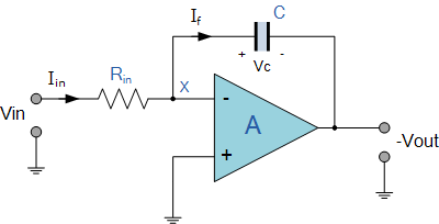
    By replacing this feedback resistance with a capacitor we now have an RC Network connected across the operational amplifiers feedback path producing another type of operational amplifier circuit commonly called an Op-amp Integrator circuit as shown below.

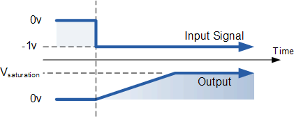
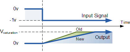
     As its name implies, the Op-amp Integrator is an operational amplifier circuit that performs the mathematical operation of Integration that is we can cause the output to respond to changes in the input voltage over time as the op-amp integrator produces an output voltage which is proportional to the integral of the input voltage.In other words the magnitude of the output signal is determined by the length of time a voltage is present at its input as the current through the feedback loop charges or discharges the capacitor as the required negative feedback occurs through the capacitor.When a step voltage, Vin is firstly applied to the input of an integrating amplifier, the uncharged capacitor C has very little resistance and acts a bit like a short circuit allowing maximum current to flow via the input resistor, Rin as potential difference exists between the two plates. No current flows into the amplifiers input and point X is a virtual earth resulting in zero output. As the impedance of the capacitor at this point is very low, the gain ratio of XC/RIN is also very small giving an overall voltage gain of less than one, (voltage follower circuit ).As the feedback capacitor, C begins to charge up due to the influence of the input voltage, its impedance Xc slowly increase in proportion to its rate of charge. The capacitor charges up at a rate determined by the RC time constant, ( τ ) of the series RC network. Negative feedback forces the op-amp to produce an output voltage that maintains a virtual earth at the op-amp’s inverting input.Since the capacitor is connected between the op-amp’s inverting input (which is at virtual ground potential) and the op-amp’s output (which is now negative), the potential voltage, Vc developed across the capacitor slowly increases causing the charging current to decrease as the impedance of the capacitor increases. This results in the ratio of Xc/Rin increasing producing a linearly increasing ramp output voltage that continues to increase until the capacitor is fully charged.At this point the capacitor acts as an open circuit, blocking any more flow of DC current. The ratio of feedback capacitor to input resistor ( XC/RIN ) is now infinite resulting in infinite gain. The result of this high gain (similar to the op-amps open-loop gain), is that the output of the amplifier goes into saturation as shown below. (Saturation occurs when the output voltage of the amplifier swings heavily to one voltage supply rail or the other with little or no control in between).

     The rate at which the output voltage increases (the rate of change) is determined by the value of the resistor and the capacitor, “RC time constant“. By changing this RC time constant value, either by changing the value of the Capacitor, C or the Resistor, R, the time in which it takes the output voltage to reach saturation can also be changed for example.

     If we apply a constantly changing input signal such as a square wave to the input of an Integrator Amplifier then the capacitor will charge and discharge in response to changes in the input signal? This results in the output signal being that of a sawtooth waveform whose output is affected by the RC time constant of the resistor/capacitor combination because at higher frequencies, the capacitor has less time to fully charge.