|
|
|
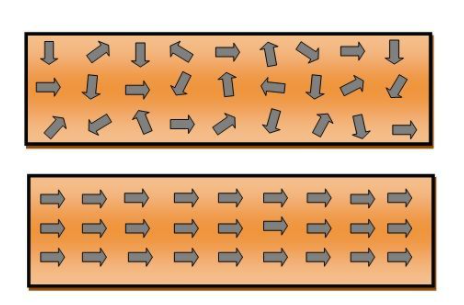
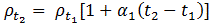 Where,ρt1 is the resistivity of material at temperature of t1o Candρt2 is the resistivity of material at temperature of t2oCα1 is temperature coefficient of resistance of material at temperature of t1o C.If the value of α1 is positive, the resistivity of material is increase.The resistivity of metals increase with increase of temperature. Means the metals are having positive temperature coefficient of resistance. Several metals exhibit the zero resistivity at temperature near to absolute zero. This phenomenon is “called the superconductivity”. The resistivity of semiconductors and insulators decrease with increase in temperature. Means the semiconductors and insulators are having negative temperature coefficient of resistance.AlloyingAlloying is a solid solution of two or more metals. Alloying of metals is used to achieve some mechanical and electrical properties. The atomic structure of a solid solution is irregular as compared to pure metals. Due to which the electrical resistivity of the solid solution increases more rapidly with increase of alloy content. A small content of impurity may increase the resistivity metal considerably. Even the impurity of low resistivity increases the resistivity of base metal considerably. For example the impurity of silver (having lowest resistivity among all metals) in copper increase the resistivity of copper.Mechanical StressingMechanical stressing of the crystal structure of material develops the localized strains in the material crystal structure. These localized stains disturb the movement of free electrons through the material. Which results in an increase in resistivity of the material. Subsequently, annealing, of metal reduces the resistivity of metal. Annealing of metal, relieve the mechanical stressing of material due to which the localized stains got removed from the crystal structure of the metal. Due to which the resistivity of metal decrease. For example, the resistivity of hard drawn copper is more as compared to annealed copper.Age HardeningAge hardening is a heat treatment process used to increase the yield strength and to develop the ability in alloys to resist the permanent deformation by external forces. Age hardening is also called “Precipitation Hardening”. This process increases the strength of alloys by creating solid impurities or precipitate. These created solid impurities or precipitate, disturb the crystal structure of metal which interrupts the flow of free electrons through metal/Due to which the resistivity of metal increases.Cold WorkingCold working is a manufacturing process used to increase the strength of metals. Cold working is also known as “Work hardening” or “Strain hardening”. Cold working is used to increase the mechanical strength of the metal. Cold working disturbs the crystal structure of metals which interfere with the movement of electrons in metal, due to which the resistivity of metal increases.Question. What is magnetic hysteresis? Enumerate the application of magnetic materials based on hysteresis characteristics Answer: The phenomenon of flux density B lagging behind the magnetizing force H in a magnetic material is known as Magnetic Hysteresis. The word Hysteresis is derived from the Greek word Hysterein means to lag behind.When the magnetic material is magnetized first in one direction and then in the other direction, completing one cycle of magnetization, it is found that the flux density B lags behind the applied magnetization force H.There are various types of magnetic materials such as paramagnetic, diamagnetic, ferromagnetic, ferromagnetic and antiferromagnetic materials. Ferromagnetic materials are mainly responsible for the generation of the hysteresis loop.
|
|
|
● Hard disk
● Audio recording devices
● Magnetic tapes
● Credit cards
Also, there exists constricted magnetic hysteresis loop substances and these are used in● Transformers
● Solenoids
● Electromagnets
● Relays
Employed in damping the angular motion of satellites in the minimal earth orbit as because of the advent of the space age.Question. Explain the effect of temperature on the magnetic behaviour of different types of magnetic materialsAnswer: All magnetic materials experience a change in flux density as their temperature increases and decreases from an ambient temperature. For example, most magnets with the exception of ferrite will actually display an increase in strength as the temperature drops and all permanent magnets (including ferrite) will lose a percentage of their performance for every degree increase. Whether this lost performance is recovered on cooling depends on the materials maximum operating temperature and the temperature the magnet is exposed to.Reversible lossReversible loss occurs for every degree rise in temperature the magnet experiences above ambient, up to its maximum operating temperature. As the magnet cools, the performance returns to the previous level.Irreversible lossWhen a magnet is heated above its maximum operating temperature but below its Curie temperature, it will experience irreversible losses in performance. This means if the magnet is then cooled, its performance will be weaker than it was before it was heated. A magnet that has experienced irreversible loss could theoretically be remagnetised back to its original strength, but this is not a cost effective process. Irreversible loss is a result of the elevated temperature reversing the magnetization of single individual magnetic domains. This means that irreversible loss happens just once; if the same thermal cycle is repeated no additional loss will occur as each individual domain can only be reversed once after it is magnetised.Permanent lossPermanent loss of magnetic performance is experienced when a magnet is heated above its Curie temperature. At this point the structure of the magnetic domains change and become self-keepering, resulting in permanent magnetic damage which cannot be repaired by remagnetisation.The Curie temperature of permanent magnetic materials is often quoted on datasheets, but when taken in isolation this is often the least useful thermal characteristic when designing an application as no design should function close to these extreme high temperatures. Therefore, other parameters such as maximum operating temperature should be considered.Neodymium magnets?The degree change in performance for a neodymium magnet depends on its shape and the design of the circuit within which it used, e.g. whether it is in ‘free space’ or whether it is connected to a steel surface. Small, thin magnets will generally be more susceptible than magnets greater in volume to rising temperatures. That considered, all neodymium magnets will lose a certain amount of performance for every degree rise in temperature even if the temperature is below their maximum operating temperature. In fact, depending on size, shape, grade and how it is used, a neodymium magnet will lose 0.08%-0.12% of its magnetic strength for every degree Celsius rise in temperature.Up to 150 degrees Celsius neodymium magnets are considered to have the best magnetic performance of all permanent magnetic materials, but when elevated to temperatures above 150 degrees Celsius their magnetic strength will be reduced below that of a magnet of the same size magnet made from samarium cobalt material. Neodymium magnets maintain their magnetic stability in very low temperatures; only at -138 degrees Celsius will their magnetic structure become affected. At this point, a neodymium magnet’s direction of magnetism will alter, resulting in a loss of performance between 10 and 20%.Standard grade neodymium magnets have a maximum operating temperature of 80 degrees Celsius. When heated above this, they will experience irrecoverable losses in performance. High temperature grades of neodymium magnets with higher maximum operating temperatures are available and these are identified by a suffix after the name of the standard grade.Samarium cobalt magnetsSamarium cobalt magnets are not as strong as neodymium magnets at room temperature but have a better temperature coefficient for both remanence (Br) and resistance to demagnetization (Hci) than neodymium magnets. For example, once the temperature exceeds 150 degrees Celsius, samarium cobalt magnets outperform neodymium magnets and standard grades of samarium cobalt (Sm2Co17) magnets will not suffer irrecoverable losses until the temperature exceeds 350 degrees Celsius.Alnico magnetsAlnico magnets are characterised by their high remanence but low coercivity, which means that they are second only to neodymium magnets in terms of magnetic strength, but are significantly more susceptible to demagnetisation by external magnetic fields and physical shock, although not by elevated temperature. In fact, of all permanent magnetic materials, alnico magnets have the greatest thermal stability only losing a fraction (0.02%) of their performance for every degree Celsius rise in temperature above ambient. Alnico magnets also have the highest maximum operating temperature of all the permanent magnet family, not suffering irreversible losses in performance until the temperature reaches 525 degrees C (alnico5).Ferrite magnetsUnique among permanent magnets, ferrite magnets actually become more resistant to demagnetization as their temperature increases. Conversely, their strength decreases as their temperature rises, albeit at a lower rate. These characteristics make them particularly popular for high temperature applications such as electric motors and generators. The intrinsic coercivity of a ferrite magnet (resistance to demagnetisation) increases by 0.4% per degree rise in temperature, while their magnetic strength decreases by 0.2% for each degree Celsius increase. Ferrite magnets can be used in temperatures up to 180 degrees Celsius before they will begin to experience irreversible losses in performance.Question. Describe the importance of single-crystalline semiconductor Answer: Mostly single crystals of semiconductors, dielectrics, metals, or alloys are produced in the process of crystallization or solidification from the melt. The rates of crystallization can reach tens of millimeters per minute. During crystallization in single crystals, structural defects can be collected that have a negative effect on the mechanical and other properties of materials. High demands for structural perfection and chemical purity of single crystals caused considerable research efforts aimed at the study and improvement of the main techniques of growing single crystals from the melt (Czochralski, Stepanov, Bridgman, Verneuil, and floating zone). Single crystals of refractory bcc metals, especially molybdenum and tungsten, are widely used in several areas of modern technology, such as nuclear energy, electronics, lighting fixtures, mainly for the manufacture of parts and devices (anodes, cathodes, etc.) working at high temperatures. A scope of single crystals of refractory metals is continuously expanding, and requirements for chemical purity of crystals, their structural quality and geometry are constantly growing. Currently, the most pure single crystals of molybdenum and tungsten, as well of a number of other refractory metals can be produced by electron-beam floating zone melting (EBFZM). However, their crystallographic perfection due to the specific features of the floating zone method with electron-beam heating, often no longer satisfies the developers of new instruments and devices. A characteristic blocky structure and a high density of dislocations make such crystals unsuitable, for example, for research of channeling high-energy particles or posing a number of other subtle physical experiments. Further increase in a degree of purity and crystallographic perfection of single crystals of refractory metals is closely related to a development of theoretical and experimental researches of crystallization processes, the development of new apparatuses and methods for producing single crystals, as well as optimization of known processes. Therefore, to obtain additional information about the laws of formation of a dislocation structure, an impact on specific parameters of crystal growth in the floating zone method seems to be a relevant scientific and technical challenge. The basis of this decision is a study of peculiarities of structural defects in single crystals grown by crystallization, which is one of the fundamental problems of solid state physics, physical chemistry, and theory of phase transitions.Shaped tungsten single crystals are used as screens of different shapes, inputs, crucibles, shapers and other products. There is considerable interest in profiled tubular shaped single crystals (primarily, of tungsten) in connection with their use in prospective designs of thermionic converters. The production of tubular tungsten single crystals from bulk cylindrical crystals by traditional machining (drilling, broaching) is extremely labor-intensive, low-tech and uneconomical. Getting such tubes pulled from the melt, for example, by Stepanov method, is impossible even for the reason that there are no available materials for the shaper. The only possibility to obtain single-crystalline tungsten tubes by crystallization from the melt is to use for this purpose the EBFZM method. Various materials can be successfully applied in industry to create structures, machine parts and devices only if they can be given in the required shape. Such shaping of crystalline materials may be done of the solid material (rolling, forging, shaping by cutting, etc.) and liquid phase (casting, welding). The shaping methods are now widely used to obtain polycrystalline products. Recently, in science and technology becoming more widely used are single crystals in the form of plates, tubes, rods of various sizes. In principle, the single-crystalline tube may be cut out from a bulk single crystal by mechanical or electrical discharge machining. However, using such kinds of processing, the single crystal will inevitably contain multiple structural defects that can alter the properties of the crystal in an unpredictable manner. For example, during the electroerosion cut of tungsten single crystals a network of cracks in the sub-surface layer occurs, and the dislocation density increases. Furthermore, such treatments are inefficient; too much waste material is usually lost. The low economic efficiency and non-technological methods have led to search for alternative methods of getting profiled single crystals. Among them are plastic deformation, epitaxial growth from the gaseous phase, crystallization from a molten solution, crystallization from the melt. Advantages of the latter forming method consist mainly in the higher productivity and better quality (because of both the structure and properties) of the final product. Crystallization from the melt provides the most perfect structure and high purity of single crystals because of the contact-less melting with no contaminating material at the front of crystallization (e.g., Czochralski method). However, due to the low stability of the capillary shaping this method can allows obtaining only products of the simplest form – the rods. Verneuil method, including plasma heating, allows obtaining single crystals of various materials in the form of tubes. It seems that the most suitable method for obtaining the tubular single crystals by crystallization from the melt is Stepanov method. The method consists in a capillary shaping of the column from the melt using a special shaper and its crystallization proceeds outside the container with the melt. The Stepanov method has a significant margin of stability and enables the profiled metal and semiconductor crystals of high quality. A float zone method can also be used for crystallization of single crystal tubes from the melt. An example of using this method to obtain tubes can be found in the monograph. In principle, the float zone methods may use any heating source, but the most suitable method to obtain the tungsten tubular single crystals with thin walls is floating zone method with electron-beam heating. Until now, by the method of EBFZM from the melt were grown the most perfect and the purest single crystals of tungsten and other refractory metals. Crystals obtained by this method typically have a cylindrical shape. EBFZM method seems to be the most promising for growing shaped single crystals of tungsten and other refractory metals in the form of tubes. Growing tubular crystals of tungsten was done on the set-up for EBFZM. Tungsten tubular feeds which were produced by CVD had an outer diameter of 16 mm and a wall thickness of 1.5 mm (a diameter of feeds varies from 10 to 22 mm). Seeds for growing single crystals were cut from the tubular cylindrical tungsten single crystals with the growth axis [111] and [001] by electro erosion, followed by removal of the damaged layer.Question. How can single crystal be produced? Explain any one technique in detail.Answer: For growing oriented single crystals of semiconductors and dielectrics, the Czochralski method became widespread. The essence of the method consists in pulling of single crystals by seeding at a surface of the melt. Although this method of capillary formation is known by its low stability, at high precision heating control and automation of pulling it allows obtaining such semiconductors as silicon and germanium which are widely used in modern technology. Bridgman method, which also refers to the crucible methods similar to Czochralski, is used in a much smaller scale and mostly for growing single crystals of low-temperature melting metals. This is due to the fact that at high temperatures there are significant difficulties in finding materials for crucibles. Another widely used technique is the Stepanov method of growing single crystals. Its difference from Czochralski consists in that the shaper is immersed into the melt, providing not only pulling cylindrical rods, but also production of a wide assortment of shaped crystals (tapes, tubes, polyhedrons, and other crystals of a complex shape). The Stepanov method has much greater margins of stability during capillary shaping than Czochralski, which accounts for its wide distribution. However, for growing single crystals of refractory metals, especially molybdenum and tungsten, the above-mentioned methods are not suitable, as the high melting temperature and high chemical reactivity of liquid refractory metals do not allow obtaining them by any crucible method. The actual process of the growth is desirable to maintain in a vacuum or in an inert gas. For refractory metals Verneuil method is also used provided with another kind of a heater as plasma. This method yielded the most by large-scale tungsten single crystals of 40 mm in diameter and weighing up to 10 kg. However, those single crystals were of poor structural quality and had high gas content, especially of a plasma gas. The most perfect single crystals of refractory metals can be obtained by electron-beam floating zone melting. The growth of these crystals is characterized by the fact that the method is a crucible-less one and a melt has no any contact with other materials. The melt is supported by forces of surface tension and the process is carried out in UHV. A phase diagram can give information on the type, number and volume fraction of phases at crystal growing from the melt. This is true only in the case when crystallization proceeds at an infinitesimal rate. In practice, a finite rate and solidification conditions are far from thermodynamic equilibrium. Thus, binary alloy solidification occurs with enrichment or depletion of solid with a dissolved component. When impurity accumulation exceeds some critical value and a temperature gradient in liquid is reduced below a critical level, there comes concentration supercooling and the interphase surface changes from cellular to dendritic. This is nonequilibrium solidification and is typical of most alloys. A main feature of such solidification is that a primary axis of dendrites is strictly parallel to a heat flow direction and interdendritic spaces are enriched with impurities. This segregation further can be partially eliminated by prolonged high-temperature annealing. In some cases, there may be precipitates of a second phase in interdendritic spaces. When crystal growth conditions are such that a part of a two-phase zone is large and a growth rate is high, so that the factor is a lot less than zero: G−V(FR)eff (1/D) ≪0, G-VFReff(1/D) ≪0, where, G the temperature gradient in fluid; V the growth rate; (FR)eff the effective solidification range; D the diffusion coefficient. Thus, there is a porosity which may occur even in growing single crystals of pure refractory metals by EBFZM. It occurs especially after the first liquid zone passage during purifying the initial PM feed and growing a single crystal from. EBFZM provides not only a given orientation of crystal growth, but also due to refining by a zone effect mainly from substitution impurities. Refining of interstitial impurities occurs mainly by vacuum evaporation, the more that the melting points of refractory metals are very high. Impurities in a growing crystal often are undesirable as adversely affecting its structure and properties. In the process of accumulation of impurities before moving crystallization front, the plane crystallization front may become unstable due to the so-called phenomenon of concentration supercooling. Impurities will greatly impair the dislocation substructure and are unevenly distributed in a radial direction and a length of the crystal along the growth axis.Question. What is Hall Effect? Derive an expression for Hall Effect in semiconductors.Answer: Hall Effect is defined as the production of a voltage difference across an electrical conductor which is transverse to an electric current and with respect to an applied magnetic field it is perpendicular to the current. Edwin Hall discovered this effect in the year 1879.Hall field is defined as the field developed across the conductor and Hall voltage is the corresponding potential difference. This principle is observed in the charges involved in the electromagnetic fields.Consider a metal with one type charge carriers that are electrons and is a steady-state condition with no movement of charges in the y-axis direction. Following is the derivation of Hall-effect: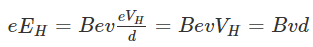 (at equilibrium, force is downwards due to magnetic field which is equal to upward electric force)Where,VH is Hall voltageEH is Hall fieldv is the drift velocityd is the width of the metal slabB is the magnetic fieldBev is a force acting on an electron
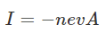 Where,I is an electric currentn is no.of electrons per unit volumeA is the cross-sectional area of the conductor
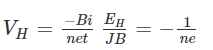 Where,
 Hall coefficient (RH) is defined as the ratio between the induced electric field and the product of applied magnetic field and current density. In semiconductors, RH is positive for the hole and negative for free electrons.
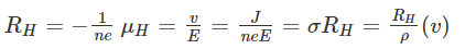 Where,E is an electric fieldv is the drift velocityRH is the Hall coefficient𝛍H is the mobility of the hole
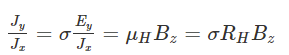 The ratio between density (x-axis direction) and current density (y-axis direction) is known as the Hall angle that measures the average number of radians due to collisions of the particles.
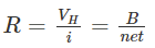 Where,R is Hall resistanceIn semiconductors, electrons and holes contribute to different concentrations and mobilities which makes it difficult for the explanation of the Hall coefficient given above. Therefore, for the simple explanation of a moderate magnetic field, the following is the Hall coefficient:
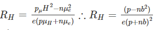 where,
● n is electron concentration
● p is hole concentration
● 𝛍e is the mobility of electron
● 𝛍H is the mobility of the hole
● e is an elementary charge
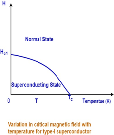
Question. What is superconductivity and its importance in engineering? Name few high-temperature superconductorsAnswer: Some materials when they are cooled, below certain temperature their resistivity get abolished means they exhibit the infinite conductivityThe temperature at which the metals change from normal conducting state to superconducting state, is called critical temperature/transition temperature. An example of superconductors, is Mercury. It becomes superconductor at 4k. In superconducting state the materials expel the magnetic field.
|
|
Type – I Superconductors | Type – II Superconductors | ||
Low critical temperature (typically in the range of 0K to 10K) | High critical temperature (typically greater than 10K) | ||
Low Critical magnetic field (Typically in the range of 0.0000049 T to 1T) | High Critical magnetic field (Typically greater than 1T) | ||
Perfectly obey the Meissner effect: Magnetic field cannot penetrate inside the material. | Partly obey the Meissner effect but not completely: Magnetic field can penetrate inside the material. | ||
Exhibits single critical magnetic field. | Exhibits two critical magnetic field | ||
Easily lose the superconducting state by low-intensity magnetic field. Therefore, type-I superconductors are also known as soft superconductors. | Does not easily lose the superconducting state by external magnetic field. Therefore, type-II superconductors are also known as hard superconductors. | ||
The transition from a superconducting state to a normal state due to the external magnetic field is sharp and abrupt for type-I superconductors.
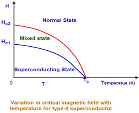
| The transition from a superconducting state to a normal state due to the external magnetic field is gradually but not shape and abrupt. At lower critical magnetic field (HC1), type-II superconductor starts losing its superconductivity. At upper critical magnetic field (HC2), type-II superconductor completely loses its superconductivity. The state between lower critical magnetic field and upper magnetic field is known as an intermediate state or mixed state.
| ||
Due to the low critical magnetic field, type-I superconductors cannot be used for manufacturing electromagnets used for producing strong magnetic field. | Due to the high critical magnetic field, type-II superconductors can be used for manufacturing electromagnets used for producing strong magnetic field. | ||
Type-I superconductors are generally pure metals. | Type-II superconductors are generally alloys and complex oxides of ceramics. | ||
BCS theory can be used to explain the superconductivity of type-I superconductors. | BCS theory cannot be used to explain the superconductivity of type-II superconductors. | ||
These are completely diamagnetic. | These are not completely diamagnetic | ||
These are also called as Soft Superconductors. | These are also called as Hard Superconductors. | ||
These are also called as Low-temperature Superconductors. | These are also called as High-temperature Superconductors. | ||
No mixed state exists in type-I Superconductors. | A mixed state exists in type-II Superconductors. | ||
Slight impurity does not affect the superconductivity of type-I superconductors. | Slight impurity greatly affects the superconductivity of type-II superconductors. | ||
Due to the low critical magnetic field, type-I superconductors have limited technical applications. | Due to the high critical magnetic field, type-II superconductors have wider technical applications. | ||
Examples: Hg, Pb, Zn,etc. | Examples: NbTi, Nb3Sn, etc. |
BASIS OF DIFFERENCE | p- TYPE SEMICONDUCTOR | n- TYPE SEMICONDUCTOR |
Group of Doping Element | In P type semiconductor III group element is added as doping element. | In n type semiconductor V group elements are added as doping elements. |
Nature of Doping Element | Impurity added creates vacancy of electrons (holes) called as Acceptor Atoms. | Impurity added provides extra electrons and is known as the Donor Atom. |
Type of impurity added | Trivalent impurity like Al, Ga, In etc. are added. | Pentavalent impurity like P, As, Sb, Bi etc. are added. |
Majority Carriers | Holes are majority carriers | Electrons are majority carriers |
Minority Carriers | Electrons are minority carriers | Holes are minority carriers |
Density of Electrons and Holes | The hole density is much greater than the electron density. nh >> ne | The electron density is much greater than the hole density. ne >> nh |
Energy level | The acceptor energy level is close to the valence band and away from the conduction band. | The donor energy level is close to the conduction band and away from the valence band. |
Fermi level | Fermi level lies between acceptor energy level and the valence band. | Fermi level lies between donor energy level and the conduction band. |
Movement of Majority carriers | Majority carriers move from higher to lower potential. | Majority carriers move from lower to higher potential. |


